

01 Hot Tech and Product Updates
In this report, there is 1 news article on the latest developments in the field of Semiconductor Thin Film – Categories. These articles have been analyzed from 2 sides: the impact of technological innovations and their effects on users. From this analysis, we have summarized the following key points:
Tech Innovations
Single-Crystal-Like Germanium Substrate
The development of single-crystal-like germanium substrates is a breakthrough in materials science. These substrates combine the desirable properties of single-crystal substrates (such as high electron mobility and uniformity) with the added benefits of flexibility and potentially lower cost.
Photoluminescence Spectrometry
This technique is used to analyze the new gallium arsenide semiconductors. It helps in understanding the electronic and optical properties of the materials, which are crucial for assessing their performance in various applications.
Epitaxial Deposition
This technique is central to the innovation described, allowing for the precise placement of molecules on a substrate to create a perfect lattice match. This method is essential for producing high-quality semiconductor films with excellent electrical and physical properties, which are critical for high-performance applications.
Roll-to-Roll Manufacturing
This manufacturing process, likened to a printing press, is noted for its cost-effectiveness and efficiency. It allows for the continuous production of semiconductor materials, which can significantly reduce costs and increase the scalability of semiconductor manufacturing.
Wide-Bandgap Semiconductors
Wide-bandgap semiconductors are crucial for devices requiring high temperature and power handling capabilities. The news article discusses the potential of these materials to replace traditional silicon-based semiconductors, highlighting their superior performance characteristics but also noting their high cost, which is a significant barrier to widespread adoption.
Flexible Substrates
The use of flexible, single-crystal-like germanium substrates represents a significant advancement in semiconductor technology. Flexibility in substrates opens up new applications in electronics, particularly in wearable and portable devices where traditional rigid substrates are unsuitable.
Product Effects
Scalability
The ability to use roll-to-roll manufacturing enables the scalable production of semiconductor materials, which is crucial for meeting the growing demand for electronic devices globally.
Light Weight
The light weight of the flexible gallium arsenide films enhances their suitability for portable electronic devices, contributing to user convenience and the functionality of modern electronic equipment.
Cost-Effectiveness
The roll-to-roll manufacturing process, along with the potential reduction in material costs due to the use of flexible substrates, contributes to the overall cost-effectiveness of the semiconductor production. This makes the technology more accessible for broader applications.
Flexibility
The flexible nature of the germanium substrates allows these semiconductor films to be used in a wider range of applications, including curved and wearable devices, expanding the potential market for these technologies.
High Performance
The epitaxial deposition technique and the use of single-crystal-like substrates contribute to the high performance of the semiconductor films. These materials are ideal for applications requiring high efficiency and reliability, such as in solar panels and advanced electronic devices.
Recommended News
Semiconductor advancement could lead to low-cost, flexible electronic devices
02 Technologies First Made Public
In this section, you will get the latest breakthroughs in four main technical directions of Semiconductor Thin Film – Categories. These technologies, first made public, represent the cutting-edge innovations and progress in the solar cell industry, showcasing the potential and direction of future developments.
Insulating Film
| Insulating Film | View 15 First Tech |
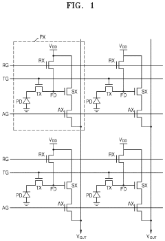
Innovation: The formation of a more uniform conductor overlapping the entire interface of a photoelectric conversion region.
Technical Effect: The technical efficacy of the patent text is that it provides a more reliable image sensor by forming a more uniform conductor overlapping the entire …
Technical Problem: The technical issues addressed in this patent text are related to the design and fabrication of an image sensor.
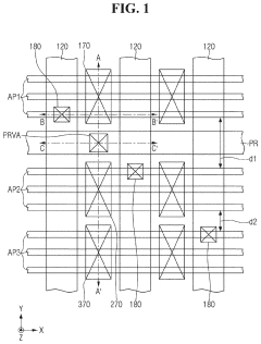
Innovation: Reduction of capacitance between contacts: the patented solution addresses the issue of high capacitance between contacts in semiconductor devices. by …
Technical Effect: The technical efficacy of the patent text is that it describes a semiconductor device that includes a substrate, active patterns, a field insulating film, ga…
Technical Problem: The technical issues addressed in this patent text are related to the design and fabrication of a semiconductor device. The specific issues addressed in the …
Optical Thin Film
| Optical Thin Film | View 13 First Tech |
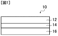
Abstract: The present invention addresses the problem of providing a liquid crystal composition that has excellent leveling properties and contains a polymer having excellent compatibility with a liquid crystal compound exhibiting reverse …
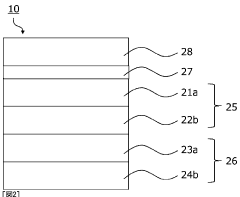
Optical layered body, layered optical film, optical article, and virtual reality display device
Abstract: The present invention addresses the problem of providing an optical layered body that produces few ghosts when used in a virtual reality display device or the like, a layered optical film that comprises the optical layered body, an …
Dielectric Film
| Dielectric Film | View 6 First Tech |

Recess filling method and plasma treatment device
Abstract: Provided is a recess filling method comprising: a step for preparing a substrate having a recess on a mounting table; a step for applying a pulsed first DC voltage to the mounting table and forming a dielectric film in the recess with pl…
Method of processing a substrate
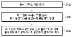
Abstract: The present invention includes the steps of preparing a substrate into a chamber where a reaction space is formed; forming a dielectric film by supplying a first process gas to the substrate under a first pressure; and a plasma process…
Semiconductor Film
| Semiconductor Film | View 4 First Tech |
Nozzle structure, semiconductor coating equipment and semiconductor coating process method
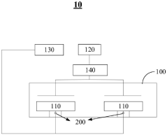
Innovation: The patent provides a nozzle structure that can automatically adjust the inlet flow of protective gas during the entire process. The nozzle structure include…
Technical Effect: The invention provides a nozzle structure that can automatically adjust the air inlet flow rate of the protective gas during the entire process, protect the …
Technical Problem: In existing semiconductor coating equipment, the heating plate is prone to oxidation problems in high-temperature environments. The existing solution is to …
A new type of organic electrochemical transistor and its preparation method and application
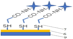
Innovation: By modifying the streptavidin-containing biomodified material layer on the gate electrode, specific recognition and binding of the target protein are achieve…
Technical Effect: This patent text describes a new type of organic electrochemical transistor, whose technical effect is to solve the technical problems in the existing …
Technical Problem: The existing Western blot detection technology has the following technical problems: it takes too long, is not stable enough, the experimental equipment is …
| Superconducting Film | View 1 First Tech |
03 Technical dynamic report in related fields
This section lists the latest updates from various fields, which will assist you to easily stay informed about the comprehensive progress of the industry and areas you might find interesting.
Semiconductor Epitaxy – Categories
Magnetic Resonance Imaging – Categories
Ultrasound Imaging – Categories
Photovoltaic Cells – Categories

