SMIC is a Shanghai-based semiconductor foundry specializing in IC fabrication from 350 nm to 7 nm nodes. Known for its scale, domestic supply-chain integration, and strategic government backing, SMIC plays a pivotal role in China’s semiconductor self-sufficiency initiative. Over the years, SMIC has built a reputation for delivering reliable manufacturing services for consumer, industrial, automotive, and communication chips.
This article offers a concise yet comprehensive breakdown of SMIC’s business focus, product offerings, and technology footprint. It also explores the company’s partnerships and recent strategic moves shaping its position in the market through PatSnap Eureka AI Agent, offering rich visual insights into technology direction, innovation strategy, and research cooperation.

Quick Company Snapshot
| Field | Details |
|---|---|
| Founded | 2000 |
| Headquarters | Shanghai, China |
| Industry | Semiconductor Foundry |
| Key Executives | Liu Xunfeng (Chairman), Haijun Zhao & Liang Mong Song (Co‑CEOs) |
| Employee Count | ~20,223 (end‑2023) |
| Key Markets | Consumer electronics, communications, automotive, industrial chips |
| Funding / Listing | Public (HKEX: 0981.HK; SSE STAR: 688981) |
| Website | https://www.smics.com |
Products & Services of SMIC
SMIC provides comprehensive foundry services across a broad node portfolio:
- Mature Nodes (350 nm–14 nm): Widely used in power ICs, sensors, microcontrollers
- Advanced Nodes (14 nm FinFET, risk 7 nm): Targeted at communication and high-end app chips
- Fab Services: 8″ & 12″ wafer fabs across Shanghai, Beijing, Tianjin & Shenzhen
- Backend Support: Packaging, testing, turnkey design support
SMIC differentiates by offering large-scale production with domestic supply chains, reducing exposure to export restrictions.
Technology Insights via PatSnap Eureka’s Company Search AI Agent
Using Eureka’s AI-driven tools, we mapped SMIC’s innovation blueprint.
1. Enterprise Technology Focus
In the dynamic landscape of corporate innovation, understanding a company’s technological priorities is crucial. PatSnap Eureka excels in dissecting this complexity by visualizing key technical terms derived from a company’s recent 5,000 patents. Through an intuitive word cloud, it aggregates and highlights the most prominent themes, making it easy to discern focal areas in R&D.
● Visualize key technical terms from recent 5,000 patents
● Show word cloud + key themes
● Explain what the focus tells us about strategic direction
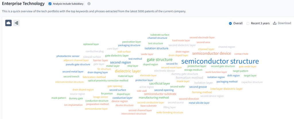
This word cloud showcases SMIC’s enterprise technology portfolio, derived from its latest patents. Key terms like “semiconductor structure,” “semiconductor device,” “gate structure,” and “dielectric layer” highlight its focus on semiconductor manufacturing tech R&D. By integrating concepts such as epitaxial layers, packaging structures, and isolation structures, SMIC gains an edge in advanced chip design, process optimization, and device fabrication. These patents back its innovation in semiconductor manufacturing, fueling advancements for more efficient and high – performance chip solutions.
2. Innovation Matrix (Tech–Application Mapping)
In the realm of corporate innovation, the Innovation Matrix within PatSnap Eureka serves as an indispensable tool for mapping the intricate relationship between technologies and their applications. By displaying patent counts across diverse application fields, it provides a quantitative overview of where a company’s innovative efforts are concentrated.
● Display patent counts across application fields
● Mention top use cases and potential white space
● Use visual (heatmap or table) if possible
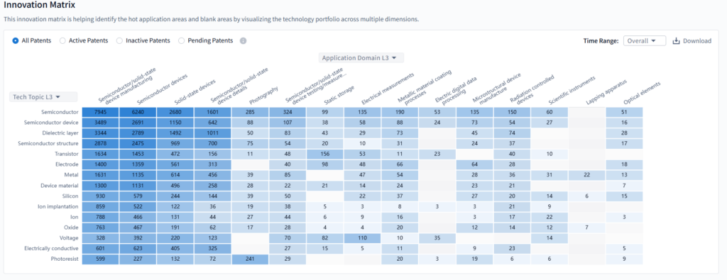
SMIC’s innovation matrix maps its patent portfolio across tech topics (Semiconductor, Dielectric layer, Transistor, etc.) and application domains (Semiconductor manufacturing, Solid – state devices, Electrical measurements, etc.). High – density areas like “Semiconductor” + “Semiconductor manufacturing” (7545 patents) reflect core R&D in chip – making fundamentals. Sparse regions, such as “Photoresist” + “Mail/paper coating” (only 3 patents), highlight potential gaps for future investment to strengthen its semiconductor – centric tech ecosystem, ensuring broader coverage in emerging manufacturing application scenarios.
3. Technology Collaboration Network
In the fast-paced world of innovation, collaboration is key. PatSnap Eureka’s Technology Collaboration Network quickly identifies SMIC’s top academic and corporate R&D partners. Using green links for joint research and purple links for joint patents, it visually maps different types of collaborations.
● Identify top academic and corporate R&D partners
● Show link types: joint patents (purple), joint research (green)
● Interpret strength of innovation partnerships
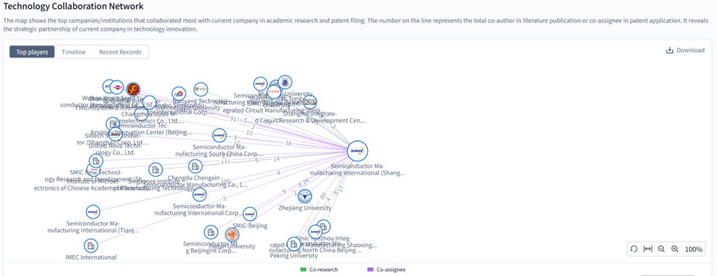
SMIC’s technology collaboration network links it with a wide range of academic institutions (like Zhejiang University) and industry players (such as research centers and tech firms). Green lines represent co – research ties, and purple lines co – assignee relationships, revealing extensive partnerships in semiconductor R&D. These collaborations help SMIC integrate diverse innovation resources, enhancing its capabilities in advanced chip manufacturing and process technology, and fueling progress in the semiconductor industry across fields like electronics, telecommunications, and consumer tech.
Recent Developments & Outlook
- SMIC is aggressively building 5 nm–14 nm capacity, targeting 5 nm risk production in 2024 .
- The company launched a Jingcheng fab using domestically sourced tools to reduce U.S. reliance .
- Q4 2024 results: Revenue rose 31.5% to $2.2 billion; Q-o-Q margin up to 22.6%; profit down 38% after heavy capex .
Looking ahead, SMIC aims to deepen domestic equipment self-reliance, ramp mature and advanced node output, and form alliances to reduce technical sanctions exposure.
For more scientific explanations of SMIC, try PatSnap Eureka’s Company Search AI Agent.