A crystal lattice is the three-dimensional, orderly arrangement of atoms, ions, or molecules in a crystalline material. This underlying framework determines the material’s physical properties, from strength and hardness to electrical conductivity and thermal behavior. In this blog, we’ll explore the fundamentals of crystal lattices, their types, structural parameters, material performance, real-world applications, and how innovations are shaping the use of lattice-based material through PatSnap Eureka AI Agent.

What is a Crystal Lattice?
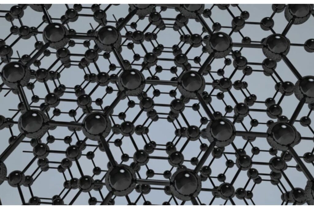
A crystal lattice refers to the periodic, repeating pattern of atoms within a crystalline solid. This arrangement defines the structure of metals, ceramics, and many semiconductors. Each point in a lattice represents the position of a constituent particle (atom, ion, or molecule), and these points collectively form the crystal structure.
Key Characteristics
- Periodic arrangement of building units in 3D space
- Unit cell is the smallest repeating unit
- Lattice parameters: edge lengths (a, b, c) and interaxial angles (α, β, γ)
- Basis: the atom or group of atoms associated with each lattice point
Composition & Properties / Performance
Chemical & Structural Data
- No fixed formula: Lattice applies to various materials (e.g., NaCl, Si, Fe)
- CAS Numbers: Depend on the constituent compound (e.g., NaCl – 7647-14-5)
Physical & Mechanical Properties
- Density: Varies by atomic mass and unit cell volume
- Melting Point: Depends on lattice bonding energy
- Thermal Conductivity: Higher in tightly packed structures (e.g., diamond)
- Hardness: Influenced by atomic bond types (ionic, covalent, metallic)
- Elasticity: Varies with lattice symmetry and defect density
Functional Characteristics
- Determines optical properties (e.g., birefringence)
- Controls bandgap behavior in semiconductors
- Affects ion migration and diffusion paths
- Defines cleavage planes for material shaping
Material Grades & Designations
While crystal lattices are a structural feature, they influence the categorization of materials based on crystal systems:
Seven Crystal Systems
- Cubic (e.g., NaCl, diamond)
- Tetragonal (e.g., SnO2)
- Orthorhombic (e.g., sulfur)
- Hexagonal (e.g., graphite)
- Trigonal (e.g., quartz)
- Monoclinic (e.g., gypsum)
- Triclinic (e.g., K2Cr2O7)
Bravais Lattices (14 Types)
Combining the 7 systems with centering types (body, face, base):
- Simple Cubic
- Face-Centered Cubic (FCC)
- Body-Centered Cubic (BCC)
- And others based on centering and symmetry
Application Landscape
Key Industries
- Electronics: Silicon’s diamond cubic lattice is essential for semiconductors
- Metallurgy: Steel’s BCC/FCC transformations define mechanical strength
- Ceramics: Ionic lattices (e.g., Al2O3) are used in insulators and abrasives
- Pharmaceuticals: Crystal polymorphs affect drug solubility and efficacy
- Nanotechnology: Crystal surfaces and planes guide nanoparticle growth
Real-World Examples
- Lithium-ion batteries: LiCoO2 has a layered hexagonal lattice
- Microchips: Use silicon wafers with precise lattice orientation
- Piezoelectrics: Lead zirconate titanate (PZT) relies on perovskite lattices
Application Trends
- Design of anisotropic materials with directional properties
- Lattice strain engineering to improve semiconductor mobility
- High-entropy alloy development using tailored crystal phases
Crystal Lattice vs Other Material Structures
| Feature | Crystal Lattice | Amorphous Solids | Polycrystalline Materials |
|---|---|---|---|
| Atomic Order | Long-range | Short-range | Mixed (grain-based) |
| Strength | Often higher | Lower | Varies by grain size |
| Examples | Diamond, NaCl | Glass, polymer gels | Metals, ceramics |
| Optical Clarity | Often transparent | May scatter light | Generally opaque |
Advantages of Crystal Lattice Structures
- Predictable Behavior: Atomic uniformity enables modeling of mechanical, electrical, and thermal responses.
- Structural Integrity: Lattices provide high resistance to deformation and stress propagation.
- Thermal and Electrical Anisotropy: Engineers can exploit directional properties for more efficient heat or charge transport.
- Mechanical Stability: Strong bonding arrangements improve resistance to thermal shock and fracture.
- Crystallographic Control: Enables tuning of catalytic activity and optical transmission through precise lattice orientation.
- Minimized Defects: Single crystals and epitaxial films can reduce grain boundaries and associated material weaknesses.
- Enhanced Functionality: Lattice symmetry affects piezoelectricity, ferroelectricity, and superconductivity in advanced materials.
Innovations & Technology
Latest Developments
- 2D Crystalline Materials: Graphene and transition metal dichalcogenides (TMDs) like MoS2 offer customizable electronic band structures.
- Quantum Lattice Simulations: AI-driven models simulate lattice vibrations, phonon interactions, and deformation under thermal stress.
- Self-Assembling Crystals: DNA-based tiles and peptide templates are enabling complex, bio-compatible lattice designs.
- Strain-Engineered Lattices: Applied strain modifies bond angles and distances to enhance mobility in transistor channels.
- Lattice Defect Engineering: Controlled introduction of vacancies, dislocations, and interstitials to tune mechanical toughness and ion transport.
- Photonic and Phononic Crystals: Engineered periodicities in dielectric or acoustic properties for precise wave manipulation.
- Programmable Metamaterials: Artificial lattices built via 3D printing and lithography for next-gen mechanical and optical functionality.
Sustainability & Environmental Impact
- Material Efficiency: Precise lattice design reduces waste in cutting and shaping
- Recyclability: Common lattice materials (e.g., metals, semiconductors) can be recovered and reused
- Energy Use: Advanced lattice structures improve energy conversion in solar cells and thermoelectrics
- Regulatory Compliance: Crystal structure analysis helps meet quality and safety standards in pharma and electronics
Conclusion
The crystal lattice is far more than a theoretical construct. It’s the blueprint for material behavior, performance, and future innovation. From electronics to biomaterials, its role in shaping properties at the atomic level enables engineers and scientists to build smarter, stronger, and more functional materials. As lattice design becomes more programmable and computationally modelable, expect new breakthroughs in materials science, energy, and health.
FAQs
It is the smallest repeating unit that defines the lattice’s overall symmetry and structure.
There are seven basic crystal systems and 14 Bravais lattice types.
Yes, through processes like annealing, which allow atoms to rearrange into a regular lattice.
It determines electron mobility, bandgap, and thermal stability—all critical for chip performance.
For more scientific explanations of crystal lattice, try PatSnap Eureka AI Agent.