
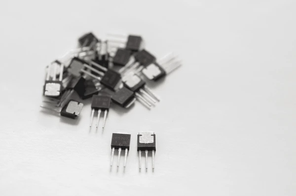
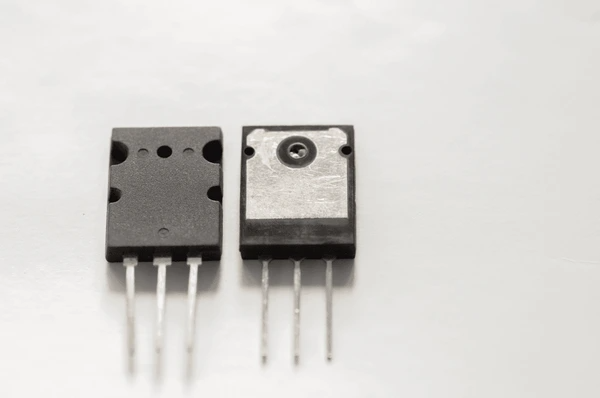
What is a MOSFET?
A MOSFET, or Metal-Oxide-Semiconductor Field-Effect Transistor, is a type of transistor used for amplifying or switching electronic signals. It is a key component in modern electronic devices and integrated circuits. The MOSFET has four terminals: a source, a drain, a gate, and a body (or substrate). The gate is insulated from the channel by a thin layer of metal oxide, which allows for precise control over the flow of current between the source and drain.
How Does a MOSFET Work?
- Channel Formation: When a voltage is applied to the gate with respect to the source, it creates an electric field that can induce a conductive channel between the source and drain regions. The type of charge carriers (electrons or holes) in the channel depends on whether the MOSFET is of the N-type (carrying electrons) or P-type (carrying holes).
- Depletion Mode vs. Enhancement Mode:
- Depletion Mode: In this mode, there is a conductive channel present even when no gate voltage is applied. Applying a gate voltage can further deplete the channel, thereby reducing the current flow.
- Enhancement Mode: In this mode, there is no conductive channel present when the gate voltage is zero. A gate voltage is required to create the channel, allowing current to flow between the source and drain.
- Gate Control: The MOSFET has practically infinite impedance due to the insulation between the gate and the channel, which makes it suitable for high-speed switching applications. The gate voltage controls the width of the conductive channel, thereby modulating the current flow between the source and drain.
Types of MOSFETs
Power MOSFETs
- Advantages: High efficiency, capable of handling high voltages and currents, suitable for power converter, motor control, and RF applications.
- Limitations: Can be sensitive to high temperatures and high power applications1.
LDMOS (Laterally-Diffused Metal-Oxide Semiconductor) Transistors
- Advantages: High gain, high power output, and high efficiency at high frequencies, commonly used in RF power amplifiers.
- Limitations: None mentioned in the provided information.
Tunnel Field Effect Transistors (TFETs)
- Advantages: Lower sub-threshold swing (< 60 mV/dec), lower leakage current, higher on/off current ratio, and better immunity to temperature variations.
- Limitations: Lower on current, which can be problematic for circuit performance.
Silicon Carbide (SiC) Power FETs
- Advantages: Suitable for high-temperature and high-power-density applications.
- Limitations: None mentioned in the provided information.
FinFETs
- Advantages: Reduced power dissipation, better voltage gain without degradation of noise or linearity, suitable for low-frequency RF applications.
- Limitations: Higher peak transconductance in planar bulk MOSFETs at high frequencies.
Key Features of MOSFETs
- n-type MOSFET: The well region is p-type doped, and the source and drain are n+ doped.
- p-type MOSFET: The reverse polarity scheme applies, with the well region being n-type doped, and the source and drain being p+ doped.
- CMOS circuits: Combine both n-MOS and p-MOS transistors to form logic gates, offering advantages in power consumption and speed.
Advantages of MOSFETs
- High Input Impedance: MOSFETs have a high input impedance, which means they do not significantly load the signal source, allowing for more accurate signal transmission.
- Low Power Consumption: They consume less power compared to bipolar junction transistors (BJTs), making them ideal for low-power applications.
- High Frequency Operation: MOSFETs can operate at very high frequencies, making them suitable for high-frequency applications such as RF amplifiers.
- Ease of Fabrication and Low Cost: MOSFETs are relatively easy to fabricate and are less expensive compared to other types of transistors, which contributes to their widespread use in digital applications.
- Improved Performance with Scaling: As MOSFETs are scaled down to smaller sizes, their performance continues to improve, enabling higher speed and density in integrated circuits.
- Versatility: MOSFETs can be used in a variety of applications, including switching, amplification, and digital logic, due to their ability to be easily controlled by voltage.
Challenges and Limitations
- Short-Channel Effects: As MOSFETs are scaled down to nanometer sizes, short-channel effects can degrade their performance and reliability.
- Subthreshold Leakage: At lower voltages, MOSFETs can experience significant leakage current, which can lead to power consumption issues.
- Temperature Sensitivity: MOSFETs can be more sensitive to temperature variations compared to some other types of transistors, which can affect their performance.
- Ambipolar Behavior: In some cases, MOSFETs can conduct current under both positive and negative gate biases, which can be a limitation in certain applications.
Applications of MOSFET
Digital Processing Applications
- MOSFETs are widely used in digital processing applications due to their ability to act as electronic switches. They are fundamental components in the construction of digital circuits, including logic gates, microprocessors, and memory devices.
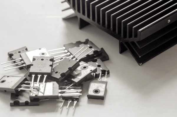
Power Electronics
- In power electronics, MOSFETs are utilized for their high current carrying capacity and voltage blocking ability. They are commonly used in applications such as switching devices in power supplies, automotive electronics, and portable electronics.
Switching Devices
- MOSFETs are employed as switching devices due to their low on-state resistance and fast switching times. They are used in applications like motor/solenoid driving and transformer interfacing.
Microprocessor Systems
- MOSFETs work in conjunction with microprocessors to facilitate the operation of circuitry. Although they often operate at different voltages, they are essential for the functionality of modern electronic systems.
Industrial Applications
- In industrial settings, MOSFETs are used in various applications, including telecommunications, industrial automation, and control systems. Their reliability and performance make them suitable for demanding industrial environments.
Consumer Electronics
- MOSFETs are used in consumer electronics such as televisions, where they require multiple power supply modules to operate efficiently. They are used for tasks such as screen operation, backlighting, and audio systems.
Latest Technical Innovations in MOSFET
Advanced MOSFET Structures
- Enhancement vs. Depletion MOSFETs: Recent research has focused on comparing the transfer characteristics of enhancement and depletion MOSFETs. Enhancement MOSFETs have shown significantly better power consumption compared to depletion MOSFETs. The power consumption of enhancement MOSFETs was found to be minimal, with values ranging from 2.2656 ± 0.37933, which is less than that of depletion MOSFETs (7.7494 ± 0.41603).
- FinFETs and Tunnel FETs: To overcome the limitations of traditional MOSFETs, innovative structures like FinFETs and tunnel FETs have been proposed. FinFETs offer improved control over the channel from three sides of the gate, providing excellent performance against Short-Channel Effects (SCEs) and a high on-to-off current ratio.
Material and Gate Engineering
- Material Engineering: Innovations in material engineering aim to improve the performance and efficiency of MOSFETs. This includes exploring new semiconductor materials with superior electrical properties.
- Gate Engineering: Techniques such as replacing the gate material with a layer of suitable receptors or etching the gate dielectric material to form nanogaps have been developed for enhanced biomolecule detection in FET-based biosensors.
Structural and Work Function Engineering
- Structural Engineering: Structural modifications, such as the FinFET structure, have been introduced to improve control over the channel and reduce SCEs.
- Work Function Engineering: Adjusting the work function of the gate material to optimize the threshold voltage and reduce leakage current.
Spacer and Gate Oxide Engineering
- Spacer Engineering: Spacers are used to improve the gate control over the channel and reduce parasitic components.
- Gate Oxide Engineering: Innovations in gate oxide engineering aim to create thinner, higher-k gate dielectrics to reduce capacitance and leakage while maintaining reliability.
To get detailed scientific explanations of MOSFET, try Patsnap Eureka.

Learn more
Multiplexor: Efficient Data Selector for Electronics
Understanding STP Cable: Shielded Twisted Pair Explained
Understanding Twisted Pair Cable: Basics, Benefits, and Uses