
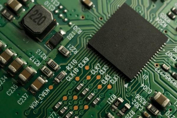
What Is PCBA?
PCBA (Printed Circuit Board Assembly) is the process of assembling electronic components onto a bare printed circuit board (PCB) to create a functional electronic product.
How PCBA Differs from PCB
Components
- PCBs are bare boards with conductive traces for connecting electronic components. They serve as the base for mounting components.
- PCBAs are fully assembled boards with electronic components like integrated circuits, resistors, capacitors, etc. soldered onto the PCB.
Assembly Process
- PCBs undergo fabrication processes like etching copper layers on a non-conductive substrate to create the conductive traces.
- For PCBAs, the assembly process involves mounting components onto the bare PCB through processes like:
- Solder paste application
- Component placement (manual or automated)
- Soldering components using a reflow oven
- Testing and inspection (e.g. in-circuit testing, automated optical inspection)
Functionality
- A PCB only provides the base and interconnections for components.
- A PCBA is a fully functional unit containing the PCB along with all the necessary electronic components to perform the intended operations.
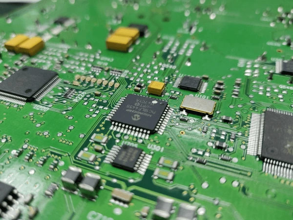
Key Components of PCBA
- Printed Circuit Board (PCB): The foundation of a PCBA, a PCB is a board made of insulating material with conductive pathways etched onto it, providing mechanical support and electrical connections for electronic components.
- Electronic Components: Various electronic components such as integrated circuits (ICs), resistors, capacitors, and connectors are mounted on the PCB. These components perform specific functions and form the core of the electronic circuit.
- Solder Joints: Solder joints are used to electrically and mechanically connect the electronic components to the conductive pathways on the PCB. Common solder joint types include through-hole and surface mount technology (SMT).
- Enclosure or Housing: Many PCBAs are enclosed in a protective casing or housing, which shields the components from environmental factors and provides structural support.
PCBA Manufacturing Process
PCB Preparation
- Bare PCBs are fabricated with conductive copper traces and pads for component mounting.
- Solder paste is applied to the pads using a stencil printer.
Component Placement
- Electronic components (active and passive) are precisely placed onto the PCB using a pick-and-place machine.
- Components can be through-hole or surface-mount technology (SMT) types.
Soldering
- Reflow soldering is commonly used for SMT components, where the PCB passes through a reflow oven to melt the solder paste and create electrical connections.
- Wave soldering can be used for through-hole components.
Inspection and Testing
- Automated optical inspection (AOI) is performed to detect defects like missing components or solder bridges.
- In-circuit testing (ICT) and functional testing are conducted to verify the PCBA’s electrical performance.
Quality Control
- Failure prevention mechanisms like solder paste inspection (SPI) and AOI are employed to ensure designated quality.
- Process parameters like solder paste printing pressure, blade angle, and speed are optimized using techniques like Taguchi methods.
Types of PCBA Assembly
- Pick-and-place machines: Components picked from feeders and placed on PCB in cycles.
- Multi-head, multi-station, turret-type, dual delivery machines.
- Solder paste printing: Stencils used to apply solder paste on PCB pads before component placement.
- Reflow soldering: PCBAs passed through an oven to melt solder and create permanent connections.
- Inspection: Automated optical inspection (AOI), solder paste inspection (SPI), in-circuit testing (ICT) to detect defects.
Benefits of PCBA
- Space Optimization and Miniaturization: PCBA allows for efficient utilization of available space by directly soldering components onto the PCB, eliminating the need for conventional screw-fastening methods. This approach improves space utilization and enables miniaturization, reducing the overall volume of the assembly.
- Improved Grounding and Signal Integrity: By soldering the PCBA directly onto the structure, the grounding characteristics of radio frequency circuits are preserved, ensuring better signal integrity and performance.
- Higher Reliability and Durability: The direct soldering of components onto the PCB eliminates the potential failure points associated with solder joints, leading to improved reliability. Additionally, the compact design and utilization of metal shielding in certain PCBA configurations enhance durability and quality.
- Cost and Time Efficiency: Automated PCBA assembly processes streamline manufacturing, reducing labor costs and production time compared to manual assembly methods. The elimination of manual fastening steps further contributes to cost and time savings.
Challenges in PCBA
- Thermal Management: The compact nature of PCBA designs and the soldering processes involved can lead to thermal challenges, such as warping or uneven soldering due to heat exposure. Proper thermal management strategies are crucial to mitigate these issues.
- Quality Control and Inspection: Ensuring consistent quality and detecting defects in densely populated PCBA assemblies can be challenging, necessitating advanced inspection techniques like automated optical inspection (AOI) and deep learning-based methods.
- Design Complexity: As electronic devices become more sophisticated, PCBA designs grow increasingly complex, requiring careful consideration of factors such as signal integrity, impedance matching, component placement, and routing. Comprehensive design rules and guidelines must be followed to ensure optimal performance.
- Environmental Compliance: PCBA manufacturing processes and materials must comply with environmental regulations and standards, such as those related to hazardous substances, energy efficiency, and recyclability. Adopting eco-friendly materials and processes is an ongoing challenge.
Applications of PCBA
Solid-State Battery Management System The PCBA integrates a solid-state relay and current shunt sensor, replacing traditional electro-mechanical contactors, fuses, and external current sensors. This enables:
- High current capability for battery management
- Improved safety through solid-state design
Monitoring and Protection Circuitry The PCBA includes monitoring, driving, and protection circuitries tailored for high current and safety-critical applications, such as:
- Voltage and current monitoring
- Overcurrent and overtemperature protection
- Energy clamping for transient events
Thermal Management Design Effective thermal management is critical for high current PCBAs. The design incorporates features like:
- Optimized board layout for heat dissipation
- Thermal vias and heat sinks
- Airflow channels for active cooling
Potential Applications This solid-state BMS PCBA can enable safer and more reliable operation in high current applications, such as:
- Electric vehicles and hybrid electric vehicles
- Renewable energy storage systems
- Uninterruptible power supplies (UPS)
- Industrial equipment and machinery
Latest Technical Innovations in PCBA
Materials and Components
- Embedded active and passive components for higher packaging density
- Nickel-metal composite metamaterials for controlling electric field effects
- Low-density packaging materials like foamed polypropylene (EPP)
Manufacturing Processes
- Build-up constructions for rigid-flex PCBs using equipment for rigid PCBs
- Packaging methods involving molding with polymer materials
- Depaneling techniques with stress minimization through hole placement
Assembly and Integration
- Printed circuit board cable clips for improved signal integrity
- Mounting structures for aligning and coupling to transmitter optical assemblies (TOSAs)
- Damping materials to dissipate kinetic energy and reduce acoustic vibration
Testing and Quality Control
- Computer vision systems based on LabVIEW for visual inspection
- Testing methods for high-speed communication applications
- Identification and location of components for disassembly
Design and Simulation
- Finite element analysis for stress minimization during depaneling
- Virtual instrument technology for efficient PCBA detection
- Control of electric field effects through design
FAQs
- What is the difference between PCB and PCBA?
A PCB is the bare board, while PCBA includes components mounted on the board, making it functional. - Can PCBA be customized for specific applications?
Yes, PCBA can be tailored to meet the design, performance, and environmental requirements of specific projects. - How is PCBA quality ensured?
Through inspection methods like AOI, X-ray testing, and functional testing during and after assembly. - What materials are used in PCBA manufacturing?
Common materials include copper (conductive layers), FR4 (insulating layer), and a variety of electronic components like ICs and resistors. - Why is PCBA critical in electronics production?
PCBA integrates components into a functional circuit, enabling devices to perform their intended tasks.
To get detailed scientific explanations of PCBA, try Patsnap Eureka.
