
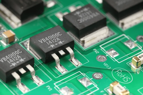
What is a Schottky Diode?
A Schottky diode is a type of semiconductor diode that is formed by the metal-semiconductor junction, as opposed to the traditional p-n junction diode. It consists of a metal in contact with a semiconductor, typically a metal in contact with a p-type semiconductor. This configuration creates a rectifying barrier that allows the diode to function as a rectifier and switching device.
How Does a Schottky Diode Work?
The working principle of a Schottky diode is based on the thermionic emission of majority carriers over the barrier formed at the metal-semiconductor junction. This results in a device that is primarily controlled by majority carriers, which allows for fast switching and low forward voltage drop.
In operation, when a forward bias is applied, majority carriers flow through the diode, allowing current to pass easily. When a reverse bias is applied, the barrier at the junction blocks the flow of carriers, preventing current flow. This behavior makes Schottky diodes suitable for applications such as RF mixing and detection, power rectification, and as clamping devices.
Key Features of Schottky Diodes
- Low Forward Voltage Drop: Schottky diodes have a significantly lower forward voltage drop compared to conventional p-n junction diodes. This can range from 0.1 to 0.4 volts, depending on the specific type of Schottky diode.
- Fast Switching Action: Due to the almost nonexistent depletion width in the metal, Schottky diodes exhibit very fast switching action, making them suitable for high-frequency applications.
- Unipolar Operation: Schottky diodes operate as unipolar devices, using majority carriers (electrons in the case of n-type semiconductors), which allows for faster switching compared to bipolar p-n junction diodes.
- High Switching Speed and Low Junction Capacitance: These characteristics make Schottky diodes suitable for high-speed circuits and radio-frequency (RF) devices.
- Rectification Mechanism: Conduction in Schottky diodes is primarily through thermionic emission of majority carriers over the barrier, which is determined by the metal work function and the semiconductor’s energy band structure.
Advantages of Schottky Diodes
- Low Forward Voltage Drop: Schottky diodes have a significantly lower forward voltage drop compared to p-n diodes, typically ranging from 0.5 V to 0.6 V at high current densities. This results in lower power loss and higher efficiency.
- High Switching Speed: Due to their majority carrier operation, Schottky diodes offer fast switching speeds, making them suitable for high-frequency applications.
- Low Junction Capacitance: Schottky diodes have much lower junction capacitance than p-n diodes, which contributes to their high switching speed and suitability for RF devices.
- Simple Structure: The metal-semiconductor junction of Schottky diodes is simpler to fabricate compared to p-n diodes, potentially reducing manufacturing costs.
- Improved Performance in Power Applications: Schottky diodes are used in power electronics due to their ability to handle high current conduction and blocking voltages with low loss.
Challenges and Limitations
- High Leakage Current: Schottky diodes typically have higher reverse leakage currents compared to pn-junction diodes, which can be a limitation in certain applications.
- Low Breakdown Voltage: The breakdown voltage of Schottky diodes is generally lower than that of pn-junction diodes, which limits their use to low-voltage applications.
- Temperature Dependence: The performance of Schottky diodes can be affected by temperature variations, which can impact their reliability and efficiency.
- Manufacturing Challenges: Achieving consistent and reliable performance in Schottky diodes can be challenging due to factors such as contact inhomogeneity and edge termination effects.
Applications of Schottky Diode
- High-Frequency Applications: Schottky diodes are well-suited for high-frequency applications due to their short reverse recovery times and low forward voltages, which result in low losses8. They are commonly used in microwave circuits for detection, circuit protection, level shifting, and switching.
- Rectenna Devices: Schottky diodes are used in rectenna devices for RF-to-DC power conversion, particularly in nanosystems. They can efficiently convert RF signals to DC power without the need for an additional matching circuit.
- Photodetector and Temperature Sensor Applications: CMOS fabricated Schottky diodes can be used for photo-detector and temperature sensor applications. They exhibit linear temperature sensing characteristics between 30°C and 80°C, making them suitable for body temperature sensors.
- Optoelectronic Applications: Schottky diodes have been integrated into optoelectronic devices, such as photodiodes. For instance, a Schottky contact was fabricated using a Cu-Al-Mn shape memory alloy and p-Si substrate, demonstrating photovoltaic behavior under various illumination conditions.
- Electrostatic Discharge (ESD) Protection: Schottky diodes are used in ESD protection circuits due to their fast switching characteristics, which help in protecting electronic circuits from voltage spikes and transient effects.
- Integrated High-Voltage Terminations: Schottky diodes can be integrated into high-voltage integrated circuits (HVICs) for applications such as driver circuits, where they can be used for voltage clamping and bootstrap purposes.
- Moving Schottky Diode Generators: A novel application involves the use of a moving Schottky diode generator that converts mechanical energy into electrical energy through lateral movement between a graphene/metal film and a semiconductor. This generator achieves high current-density output and has potential for portable energy sources
Latest Technical Innovations in Schottky Diode
Material Innovations
- Titanium Nitride and Silicidation Prevention: The use of titanium nitride in Schottky diode fabrication prevents unwanted silicidation, thereby improving diode stability and performance. This material choice allows for a tunable barrier height, making the diode more versatile for various applications.
- Graphene-based Heat Spreader: The integration of reduced graphene oxide (RGO) as a heat spreader in Schottky diodes reduces leakage current by two orders of magnitude, especially at high operating temperatures. This innovation enhances efficiency and reliability under extreme conditions.
- Dual Metal and Barrier Layer Structures: Innovations in dual metal Schottky diode structures, such as the use of PtSi, TiSi2, and Ti, allow for the formation of barrier layers that can be optimized for desired performance and reliability characteristics. The ability to remove or reform these layers during fabrication further enhances diode performance.
Structural Enhancements
- Trench and Guard Ring Structures: The incorporation of trench MOS Schottky barrier diode structures and guard rings in the cathode region improves performance, reliability, and stability. These structures help in managing electrical field distribution and reducing leakage currents.
- Edge Termination and Doping Modifications: Improved edge termination techniques and doping modifications, such as the periodic inclusion of highly doped thin layers, significantly enhance the forward performance of Schottky diodes. These modifications can increase forward current density by factors of 10-17, and are particularly beneficial in high-power applications.
Manufacturing Process Improvements
- CMOS Compatibility and Low Leakage: Innovations in manufacturing processes aim to improve the compatibility of Schottky diodes with CMOS technology, ensuring low reverse leakage and good area efficiency. These improvements are achieved without compromising the existing IC manufacturing steps, thus maintaining cost-effectiveness.
- Oxide Semiconductor and High-k Dielectric Materials: The development of metal-oxide-semiconductor (MOS) Schottky diodes utilizes oxide layers to increase barrier heights and reduce leakage currents. Recent advances involve the use of high-k dielectric materials and thin-film nanostructures, which further enhance performance for applications like photodetectors and sensors.
To get detailed scientific explanations of schottky diodes, try Patsnap Eureka.

Learn more
Multiplexor: Efficient Data Selector for Electronics
Understanding STP Cable: Shielded Twisted Pair Explained
Understanding Twisted Pair Cable: Basics, Benefits, and Uses