Lam Research stands as a global powerhouse in the semiconductor manufacturing equipment sector. Since its establishment, it has been at the forefront of enabling the production of ever – smaller, more powerful microchips. Specializing in plasma etching, deposition, and wafer cleaning technologies, the company plays a pivotal role in shaping the infrastructure of the modern digital world. From powering advanced consumer electronics to fueling breakthroughs in artificial intelligence and data centers, Lam Research’s innovations are integral to the continuous evolution of semiconductor technology, driving progress across industries and empowering the next generation of technological advancements.
This article offers a comprehensive look into Lam Research’s organizational design, technological expertise, IP portfolio, financial trajectory, and strategic vision—amplified by PatSnap Eureka AI Agent powerful analytical capabilities to explore innovation patterns, patent strengths, and competitive intelligence.

Company Overview
| Feature | Description |
|---|---|
| Company Name | Lam Research Corporation |
| Founded | 1980 |
| Headquarters | Fremont, California, USA |
| CEO | Tim Archer |
| Employees | ~17,200 (2024) |
| Industry | Semiconductor Equipment Manufacturing |
| Ticker | NASDAQ: LRCX |
| Core Offerings | Etch, Deposition, Clean, and Equipment Services |
| Main Clients | TSMC, Samsung, Micron, Intel, SK Hynix |
| Manufacturing Footprint | U.S., Korea, Taiwan, Japan, China |
Corporate Structure
| Division/Unit | Core Function |
|---|---|
| Etch Products Group (EPG) | Delivers leading-edge plasma etch tools for logic and memory applications |
| Deposition Product Group | Focuses on Chemical Vapor Deposition (CVD), Atomic Layer Deposition (ALD) |
| Clean Systems Group | Provides post-etch cleaning solutions for wafers |
| Customer Support Business Group | Offers spares, upgrades, predictive maintenance, and analytics |
| Global Operations | Manages supply chain, logistics, and manufacturing optimization |
| Corporate Strategy & Development | Drives investment, partnership, and long-term innovation alignment |
Business Model and Services
Lam Research operates a capital equipment and lifecycle services model targeting Integrated Device Manufacturers (IDMs) and Foundries. The company integrates its tools into clients’ advanced process nodes, building collaborative partnerships to solve scaling and material challenges.
Key Service Verticals:
- Equipment sale (etch, deposition, clean)
- Equipment upgrades and refurbishment
- Predictive diagnostics and real-time analytics
- Process development collaboration
- Ecosystem partnerships (e.g., ASML, imec)
Revenue Breakdown (Est. 2024):
- Etch Systems: 40–45%
- Deposition Systems: 25–30%
- Services and Support: ~30%
Innovation & Technology
As semiconductor devices approach physical scaling limits below 5nm—and enter the era of Gate-All-Around (GAA), backside power delivery, and 3D logic—Lam Research plays a mission-critical role in enabling atomic-level control over materials, geometries, and process uniformity.
Lam’s core innovation strategy is centered around three pillars:
- Atomic Precision: Manipulating material at the angstrom level
- Selective Processing: Enabling ultra-targeted deposition and etch without masks
- Integrated Intelligence: Embedding data analytics into fabrication hardware
Using PatSnap Eureka AI Agent, technology and R&D teams can map Lam’s innovation footprint across these pillars, revealing dense clusters of patents, strategic shifts in materials, and competitive claims in key domains like HARC (High Aspect Ratio Contact), selective etch, and atomic-layer metrology.
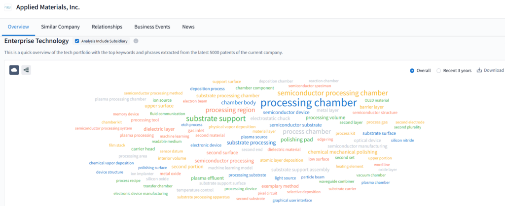
Patent-Derived Technology Themes
1. Plasma Processing and Reactor Chambers
Lam Research’s legacy lies in plasma etching—a technique that uses ionized gases to sculpt microscopic features. This is crucial for patterning FinFET gates, NAND channels, and DRAM capacitor stacks.
- Keywords: plasma processing system, plasma chamber, rf signal, process gas, remote plasma
- Notable Value: These patents govern how plasma interacts with surfaces while ensuring selectivity and feature integrity, particularly in deep narrow trenches.
Eureka reveals Lam’s concentrated IP around multi-zone plasma control, which allows precise tailoring of ion energies across substrates—key to consistent etch profiles at high aspect ratios.
2. Atomic Layer & Selective Deposition
Unlike traditional deposition, ALD (Atomic Layer Deposition) builds films atom-by-atom, offering extreme uniformity and conformality—ideal for 3D NAND, logic interconnects, and spacer-defined patterning.
- Keywords: atomic layer deposition, selective deposition, tin oxide film, chemical vapor deposition
- Key Innovations: Lam’s breakthroughs include area-selective ALD and plasma-enhanced ALD (PEALD) processes that prevent unwanted deposition, enabling new design flexibility.
Using Eureka, users can trace Lam’s innovation lineage from early tin oxide nucleation layers to its latest self-aligned barrier films, critical for extending Moore’s Law through 3D scaling.
3. Semiconductor Device Enablers
This theme focuses on substrate handling, chamber integration, and feature definition at nanoscale resolution. Patents in this domain support precision in multi-patterned layers and high-aspect structures.
- Keywords: substrate processing system, high aspect ratio feature, etch feature, semiconductor wafer
- Commercial Value: These technologies enable chipmakers to etch deep vertical structures (e.g., 256+ layers in 3D NAND) while minimizing sidewall damage or distortion.
Eureka’s graph clustering shows a high co-occurrence between “etch feature” and “substrate support,” signaling Lam’s dominance in systems where mechanical and plasma dynamics converge.
4. Thermal and Control Engineering
Temperature and electrostatic control are pivotal for maintaining plasma uniformity and preventing wafer warping. Lam has invested in multi-zone temperature management and RF tuning systems.
- Keywords: heating element, temperature sensor, electrostatic chuck, process module
- Application: Essential in processes such as ALD/etch cycling and dual-damascene metallization.
Eureka allows comparative analysis of Lam’s thermal architecture patents versus competitors like Applied Materials—providing insight into claims depth and thermal compensation strategies.
5. Process Integration and Gas Flow Optimization
Controlling gas flow and reactant distribution within confined spaces ensures layer uniformity and eliminates defects. Lam’s designs use showerhead injectors and annular flow systems to distribute gases evenly.
- Keywords: second inlet, carrier ring, shower head, gas distribution device, purge gas
- Innovation Significance: Patents in this space contribute to process repeatability, chamber cleaning efficiency, and cycle-time reduction.
Sustainability and Corporate Responsibility
Lam is committed to reducing its environmental footprint via:
- Energy Efficiency: >25% reduction in tool energy per wafer pass (2019–2024)
- GHG Reduction: Transitioning to alternative chemistries (e.g., replacing NF3 with remote plasma N2/H2)
- Circular Economy: Refurbished tool program, spare parts remanufacturing
- Diversity & Inclusion: “Inclusion First” program supports global DEI goals
Strategic R&D Focus Areas (2025 Onward)
| Area | Lam’s Investment Focus |
|---|---|
| EUV Compatibility | Plasma strip and post-litho clean systems for ultra-thin resist layers |
| GAA/CFET Nodes | ALD spacer and liner processes, sub-nanometer etch modulation |
| 3D Memory Expansion | High-aspect etch, low-k dielectric deposition, pitch reduction |
| Backside Power Delivery | Ultra-thin wafer etch, wafer bonding support systems |
| Green Manufacturing | Low-global warming process gases, energy-efficient RF matching systems |
Market Presence and Financials
| Metric | 2024 Estimate |
|---|---|
| Annual Revenue | ~$18.5 billion |
| Net Income | ~$5.3 billion |
| R&D Investment | ~$2 billion (~11% of revenue) |
| Free Cash Flow Margin | ~25% |
| Top Regions | Taiwan, South Korea, China, U.S. |
| Market Share (Etch) | 50–55% globally |
Lam’s strength lies in deep customer engagement and strategic node-aligned development, which has earned preferred vendor status at TSMC and Micron.
Competitor Analysis
| Company | Core Focus | Differentiator vs. Lam |
|---|---|---|
| Applied Materials | Broad process suite (PVD, CVD, Etch) | Larger ecosystem but less specialized in plasma |
| Tokyo Electron | Strong Asia fab integration | Coater/developer dominance |
| ASML | EUV Lithography Systems | Complementary partner not direct competitor |
| KLA Corporation | Process control/metrology | Yield engineering not process module |
| AMEC (China) | Local plasma tools | Cost-sensitive but limited innovation footprint |
Eureka allows granular benchmarking—such as comparing Lam’s etch patents to AMAT’s patterning solutions across geographies, process families, or citation depth.
PatSnap Eureka AI Agent Capabilities
With PatSnap Eureka AI Agent, professionals can:
- Map Patent Families: Track innovation clusters around atomic layer etch or 3D NAND
- Assess IP Strength: Analyze Lam’s citation influence, claim breadth, and legal stability
- Compare Across Peers: Benchmark Lam vs. Applied Materials or TEL in substrate processing
- Detect Strategic Shifts: Spot emerging investments in tin oxide or carbon-free processes
- Predict Technology Paths: Use AI to correlate patents with upcoming foundry roadmaps
Conclusion
Lam Research is more than a tool supplier—it’s an atomic innovation partner to the world’s most advanced chipmakers. From enabling vertical NAND scaling to pioneering dry development for EUV, Lam’s technologies are foundational to modern electronics.
To explore Lam’s full technology DNA and stay ahead of the semiconductor innovation curve, PatSnap Eureka’s Company Search AI Agent provides unmatched visibility into IP strategy, competitive trends, and future market direction.