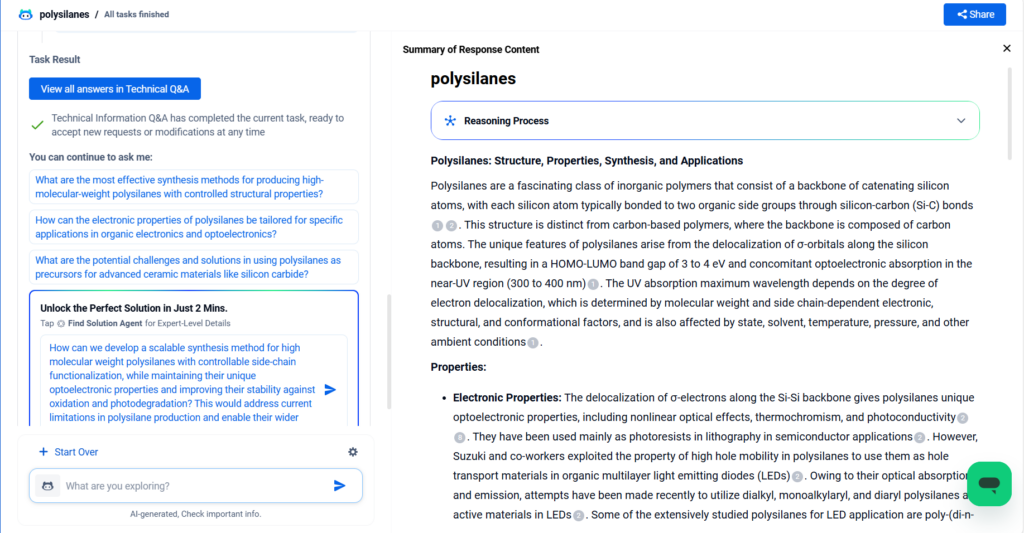
Polysilanes are a unique class of silicon-based polymers with repeating Si-Si bonds in their backbone. These materials exhibit distinctive properties, such as high thermal stability and UV absorption, making them promising for advanced applications in microelectronics, optoelectronics, and ceramics. This blog explores polysilane’s composition, properties, applications, grades, and technological innovations—while illustrating how PatSnap Eureka AI Agent reveals key insights in polysilane R&D.

What is Polysilane?
Polysilanes are organosilicon polymers composed of alternating silicon atoms typically bonded to organic side groups. Their σ-conjugated Si-Si backbone provides unique electronic and optical properties, distinguishing them from conventional organic polymers. The general formula is (R2Si)n, where R denotes alkyl or aryl groups.
Composition & Properties / Performance
Chemical Composition
- General Formula: (R2Si)n
- CAS Number: Varies; e.g., 113957-97-0 for polymethylsilylene
- Molecular Weight: Ranges from a few thousand to over 100,000 Da
Physical & Mechanical Properties
- Density: ~1.0–1.3 g/cm³ (depending on side groups)
- Melting Point: Amorphous—typically decomposes >300°C
- Refractive Index: ~1.5–1.7
- Glass Transition Temperature (Tg): Typically 100–150°C
- Solubility: Soluble in organic solvents (e.g., toluene, THF)
Functional Properties
- High thermal and oxidative stability
- Strong UV absorption and photodegradation resistance
- Semiconductor-like σ-conjugated backbone for charge transport
- Precursor to silicon carbide (SiC) ceramics
Material Grades & Designations
Common Variants
- Polymethylsilylene (PMS): High thermal resistance
- Polydimethylsilylene: Flexible and optically transparent
- Polyphenylsilylene (PPS): Better oxidative stability and UV absorption
Cross-Reference Table
| Grade | Structure | Key Feature |
|---|---|---|
| PMS | (CH3)2Si | SiC precursor |
| PPS | (C6H5)2Si | UV-blocking & optical stability |
| Copolymeric blends | Mixed R-groups | Tunable solubility/performance |
Application Landscape
Core Industries
- Electronics: Dielectric films, photoresists, insulating coatings
- Photonics: UV-blocking layers, light-harvesting materials
- Coatings: Protective films on optics and sensors
- Ceramics: Precursor for high-performance SiC fibers and composites
- Biomedical: Drug delivery, biodegradable photoreactive implants (early research)
Real-World Examples
- Polysilane coatings protect semiconductor wafers during etching.
- PMS-derived fibers are used in thermal barrier applications.
- UV-absorbing polysilane films are explored in solar cells and OLEDs.
Emerging Trends
- Development of polysilane-inorganic hybrid nanocomposites
- Use of laser-assisted patterning for photonic circuit fabrication
- Application in printable electronics and flexible semiconductors
- Integration with organic semiconductors to enhance charge mobility
- Use as carrier materials in photodynamic therapy systems
Polysilane vs Other Similar Materials
| Feature | Polysilane | Polysiloxane | Polyethylene |
|---|---|---|---|
| Backbone Type | Si-Si | Si-O | C-C |
| Thermal Stability | High | Moderate | Low |
| Optical Properties | UV absorbing | Transparent | Non-functional |
| Ceramics Precursor | Yes | No | No |
Advantages of Polysilane
- Thermal resilience: Polysilanes remain stable at temperatures above 300°C, making them suitable for extreme conditions.
- Photostability: Their ability to absorb ultraviolet light without degrading extends product life in UV-exposed applications.
- Solution processability: Polysilanes dissolve in common organic solvents, making them ideal for spin-coating and inkjet printing techniques.
- Ceramic conversion: Upon pyrolysis, polysilanes convert to high-yield SiC ceramics, useful in aerospace and structural composites.
- Electronic applications: Their σ-conjugated backbones provide useful pathways for charge transport, crucial for semiconducting and light-emitting materials.
- Molecular tunability: By adjusting the side groups, chemists can fine-tune the material’s solubility, thermal properties, and optical behavior.
- Crosslinking potential: They can be photochemically or thermally crosslinked, enhancing durability and mechanical strength.
Innovations & Technology
Recent Developments
- Photo-patternable polysilanes: These allow high-resolution lithography for microelectronic devices by using deep UV exposure to create fine features.
- Preceramic polymers: Engineered for controlled ceramic microstructure formation, offering low-shrinkage and high-yield SiC production.
- Hybrid nanocomposites: Blending polysilanes with metal oxides (e.g., TiO2, ZnO) has enhanced their thermal conductivity and UV shielding performance.
- Nanostructured films: Thin films with nanostructured interfaces show promise in photodetectors, light-emitting diodes, and perovskite solar cells.
- Flexible devices: Research shows that polysilane-based substrates can support printable electronics with mechanical flexibility and high charge mobility.
- High-k dielectrics: Polysilane derivatives with high dielectric constants are being tested for gate dielectrics in next-gen transistors.
- Photodynamic therapy carriers: Some polysilanes are under evaluation as light-activated carriers for targeted cancer treatment.
Sustainability & Environmental Impact
- Recyclability: Difficult due to crosslinking; often used as permanent materials
- Environmental safety: Generally inert and low-toxicity but not biodegradable
- Energy efficiency: Used in energy-conserving applications (e.g., UV filters, SiC ceramics)
- Compliance: Materials can meet RoHS and REACH guidelines with formulation controls
PatSnap Eureka AI Agent Capabilities
- Analyzes patent activity in advanced ceramics and UV-blocking materials
- Visualizes innovation clusters in polysilane composites
- Tracks competitors developing high-yield SiC precursors
- Maps white space for next-gen optoelectronic applications
Conclusion
Polysilanes offer a rare combination of thermal stability, photoreactivity, and electronic performance. Their role as precursors for ceramics and functional coatings positions them at the intersection of materials science and engineering. With tools like PatSnap Eureka, researchers can monitor innovation trends, identify niche opportunities, and accelerate the development of next-generation polysilane materials.
FAQs
Polysilanes have a silicon-silicon (σ-bonded) backbone, unlike most organic polymers.
Yes. They’re applied in dielectric coatings, photoresists, and printed electronics.
Absolutely. Upon pyrolysis, they produce silicon carbide (SiC) with high ceramic yields.
No. They’re generally not biodegradable but are stable and inert in most environments.
For more scientific explanations of polysilanes , try PatSnap Eureka AI Agent.