SK hynix Inc., headquartered in Icheon, South Korea, is one of the world’s foremost memory semiconductor manufacturers. Specializing in DRAM, NAND Flash, and CMOS image sensors, the company plays a foundational role in enabling data-intensive technologies from smartphones to data centers.
This article delivers a comprehensive view of SK hynix’s corporate profile, product innovation, financial strength, and global position—enhanced with IP insights powered by the PatSnap Eureka AI Agent, which allows you to explore SK hynix’s deep patent landscapes and R&D trends with precision.

Company Overview
| Key Attribute | Details |
|---|---|
| Founded | 1983 (as Hyundai Electronics Industries Co., Ltd.) |
| Headquarters | Icheon, Gyeonggi Province, South Korea |
| CEO | Kwak Noh-Jung |
| Global Rank | 2nd largest DRAM and 3rd largest NAND Flash producer globally |
| Employees | ~36,000 (2024) |
| Key Markets | South Korea, USA, China, Japan, Europe |
| Key Subsidiaries | Solidigm (U.S.), SK hynix America, SK hynix Japan |
Corporate Structure
| Business Segment | Description |
|---|---|
| Memory Solutions | DRAM and NAND Flash memory for mobile, server, consumer, and embedded use |
| Storage Solutions | SSDs and enterprise storage systems (via Solidigm) |
| CMOS Image Sensors | Imaging solutions for mobile and industrial use |
| Packaging & Test Services | Advanced chip packaging and testing for internal and OEM customers |
| R&D & Licensing | Patent licensing, next-gen memory (e.g., HBM, PIM) |
Products and Services
SK hynix has developed a diversified and future-ready portfolio of semiconductor products that support the digital transformation across industries such as mobile, data center, AI, automotive, and consumer electronics.
DRAM Solutions
SK hynix is a global leader in DRAM, powering everything from smartphones to high-performance computing. Key DRAM products include:
- DDR5 (Double Data Rate 5): Offers significantly higher bandwidth and energy efficiency compared to DDR4, ideal for AI/ML training and HPC applications.
- LPDDR5/5X (Low Power DDR): Designed for mobile and automotive platforms, providing high-speed and low-power features.
- GDDR6 (Graphics DRAM): Optimized for GPUs in gaming, AI acceleration, and AR/VR applications.
- HBM3 (High Bandwidth Memory): A premium stacked memory designed for AI chips and large-scale compute systems. SK hynix is the world’s first supplier of commercial HBM3.
NAND Flash Memory
SK hynix produces advanced 3D NAND (V-NAND) flash memory used in SSDs, embedded systems, and IoT devices.
- 176-layer and 238-layer NAND: Industry-leading layer stacking for increased density and improved speed.
- QLC (Quad-Level Cell): Enables higher storage capacity with lower cost per bit, ideal for hyperscale storage solutions.
- PCIe Gen4/Gen5 SSDs: High-performance SSDs for client and enterprise markets.
- Embedded UFS: Universal Flash Storage for smartphones and tablets.
CMOS Image Sensors (CIS)
SK hynix is a rising player in the image sensor market, providing high-resolution, low-noise imaging solutions for:
- Smartphones (up to 64MP resolution)
- Automotive cameras
- Surveillance and industrial inspection
- AI-enabled vision systems
Its sensors incorporate backside illumination (BSI), stacked architecture, and on-chip AI logic for enhanced performance in low-light and high-frame-rate environments.
Solidigm Enterprise SSDs
Following the acquisition of Intel’s NAND and SSD business, SK hynix established Solidigm as its enterprise storage arm.
- Data Center SSDs: PCIe Gen4 NVMe SSDs with industry-best performance-per-watt.
- Edge Storage: Storage solutions optimized for edge computing and real-time analytics.
- Firmware-Level Optimization: AI-driven performance tuning for workload-specific use cases.
Advanced Packaging & System Integration
SK hynix also provides advanced backend solutions that boost chip performance and density:
- TSV (Through-Silicon Via) and 2.5D/3D IC packaging
- Multi-chip Packages (MCP) combining DRAM + NAND
- Wafer-Level Packaging (WLP) for ultra-thin designs
Business Model
SK hynix operates a B2B (business-to-business) model, selling its semiconductor products to global OEMs and hyperscalers. Key aspects include:
- Vertical Integration: From fabrication to packaging and testing
- Design-to-Manufacture Synergy: Full-stack chip design and foundry execution
- Global Sales Network: Extensive footprint in Asia-Pacific, North America, and EMEA
- R&D-Driven IP Licensing: Leveraging patents for technology partnerships and standard-setting
Market Position
SK hynix holds a top-tier position in global memory markets:
- #2 in DRAM (behind Samsung)
- #3 in NAND Flash (after Samsung and Kioxia)
- Stronghold in high-performance memory: HBM3, DDR5, and AI/edge-compute chips
- Strategic customers: Apple, Microsoft, Amazon, NVIDIA, Meta, Huawei
Its acquisition of Intel’s NAND and SSD business (now Solidigm) solidified its presence in enterprise storage.

Innovation & Technology
SK hynix’s R&D strategy is deeply integrated with its business roadmap, focusing on performance-per-watt, AI compatibility, storage density, and heterogeneous integration.
Core Innovation Areas
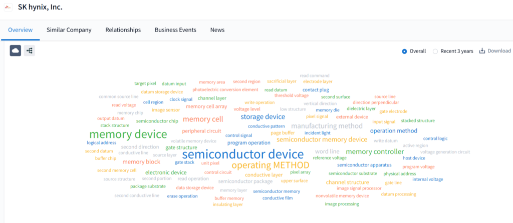
With support from PatSnap Eureka AI Agent, we can identify key innovation fields through its patent cloud and technology clustering:
| Innovation Domain | Highlights |
|---|---|
| Memory Architecture | Multi-bit memory cells, 3D stacking, buffer memory systems |
| Data I/O | Page buffer innovations, high-speed read/write, data bus control |
| Voltage Optimization | Reference voltage tuning, low-leakage voltage, voltage generation circuits |
| AI Acceleration | Processing-in-memory (PIM), in-memory computing structures |
| Sensor Integration | Photoelectric conversion layers, pixel arrays, image signal processing |
| Packaging | Die stacking, TSV, conductive interconnects, thermal management materials |
Processing-In-Memory (PIM)
SK hynix is a front-runner in PIM technology, which enables AI processing directly within memory modules. PIM reduces the need to transfer data to the CPU/GPU, significantly boosting AI inference efficiency.
- Deployed in HBM-PIM modules for AI data centers.
- Compatible with existing computing infrastructures.
- Reduces power consumption by up to 50% in certain AI workloads.
HBM3 and Beyond
SK hynix introduced HBM3, the third-generation high bandwidth memory, capable of:
- 800 GB/s per stack bandwidth
- AI and HPC-ready performance
- Thermal-aware and power-optimized stack designs
- Integration with cutting-edge AI accelerators like those from NVIDIA, AMD, and Intel
Semiconductor Process Innovation
- EUV (Extreme Ultraviolet) Lithography is now adopted in DRAM and NAND processes to push scaling limits.
- 176L and 238L NAND use charge trap flash (CTF) technology for higher endurance and lower cross-talk.
- Backend process automation includes AI-based defect analysis, predictive maintenance, and digital twin modeling.
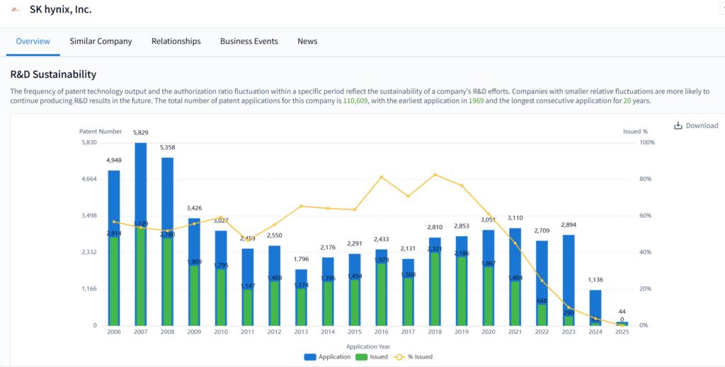
IP Portfolio Insights
PatSnap Eureka AI Agent reveals:
- Over 27,000+ patent families related to memory and semiconductor devices.
- High-density filings in semiconductor memory device, read/write operation, bit line, channel structure, and insulating layer.
- Collaboration-linked filings with top universities and global tech partners.
- Strong patent activity in Korea, U.S., China, Japan, and Europe—indicating global R&D footprint.
Market Presence and Financials
| Metric | Value (2024) |
|---|---|
| Revenue | ~$29.5 billion USD |
| R&D Investment | ~$3.5 billion USD (~12% of annual revenue) |
| Operating Margin | ~13% (rebounded after 2023 semiconductor downturn) |
| CapEx | ~$10 billion (focused on M16 fab and U.S. expansion) |
| Key Facilities | Icheon (Korea), Cheongju (Korea), Dalian (China), Oregon (USA – Solidigm) |
| ESG Focus | Carbon-neutral roadmap, eco-friendly fabs, digital twins for energy mgmt. |
Competitors Analysis
| Company | Focus Area | Competitive Edge |
|---|---|---|
| Samsung | Full-stack semiconductor giant | Scale, vertical integration, foundry leadership |
| Micron | DRAM/NAND focus | U.S. base, AI-optimized memory chips |
| Kioxia | NAND specialty (ex-Toshiba Memory) | 3D NAND innovation, strategic partnerships with WD |
| Intel (pre-Solidigm) | NAND/Optane storage | Enterprise SSD IP, later transferred to SK hynix |
| Western Digital | NAND storage and HDD | Synergy between HDD/NAND, joint venture with Kioxia |
PatSnap Eureka AI Agent Capabilities
SK hynix’s massive IP library presents a strategic intelligence opportunity. Using PatSnap Eureka AI Agent, users can:
- Map out technology clusters (HBM, PIM, 3D NAND, image sensing)
- Identify emerging innovation signals
- Compare citation density and patent strength with rivals
- Discover market trends from SK hynix’s forward-looking patents
- Extract inventor-level insights and global patent family dynamics
Eureka transforms dense patent data into actionable competitive insights—enabling semiconductor strategists, investors, and engineers to stay ahead in this capital-intensive, innovation-driven industry.
Conclusion
SK hynix remains a central player in the global semiconductor ecosystem, known for its technological finesse in memory, imaging, and system integration. By combining a robust patent strategy with high-yield production and strategic acquisitions, it is well-positioned to fuel the data-driven economy.
With the PatSnap Eureka AI Agent, businesses and analysts can unlock deep R&D and IP intelligence on SK hynix—transforming how you explore semiconductor innovation at scale.
FAQs
No. SK hynix is an independent company, part of the SK Group, competing with Samsung in the memory chip market.
Often tied to memory chip market cycles (oversupply → price drops), macroeconomic trends (weak demand), or tech industry slowdowns.
High R&D costs for advanced memory tech, supply – demand swings (shortages raise prices), and its premium position in high – performance chips.
In specific segments (e.g., certain DRAM niches) it competes closely, but Samsung remains a top rival; overall market leadership varies by category.
Primarily self – fab or uses partner foundries for some processes, but TSMC isn’t a core supplier (focus on in – house/strategic partners).
By leveraging the PatSnap Eureka’s Company Search AI Agent, you can unlock actionable insights into SK hynix’s cutting-edge memory and storage innovations—empowering your organization to stay ahead in the era of AI-driven computing and high-performance semiconductor technologies.