Atomic Layer Deposition (ALD) has emerged as one of the most critical thin-film deposition techniques in the semiconductor industry. As chip designs continue to shrink and require ultra-thin, conformal layers of materials with atomic-level precision, ALD provides a solution that traditional deposition methods cannot match.
Curious about Atomic Layer Deposition (ALD) in semiconductors? Eureka Technical Q&A explains how ALD enables ultra-thin, precise coating of materials at the atomic level — helping improve chip performance, energy efficiency, and device miniaturization in modern electronics.

This article explains what Atomic Layer Deposition is, how it works, and why it is essential for advanced semiconductor manufacturing.
What is Atomic Layer Deposition (ALD)?
Atomic Layer Deposition (ALD) is a vapor-phase thin-film deposition process that allows materials to be deposited in ultra-thin layers — one atomic layer at a time. It is a specialized form of Chemical Vapor Deposition (CVD) but offers greater control over film thickness, uniformity, and conformality.
ALD is vital in semiconductor fabrication, where precise control over thin-film characteristics is critical for the performance of transistors, capacitors, memory devices, and advanced logic circuits.
How Atomic Layer Deposition Works: Step-by-Step Process
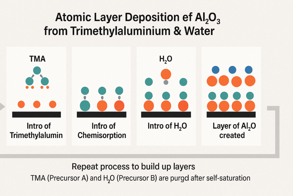
ALD operates based on a sequential, self-limiting chemical reaction process. Unlike traditional deposition methods that apply material continuously, ALD introduces precursor gases in separate pulses, allowing atomic-scale control of film growth.
Step 1: Precursor A Exposure
The first precursor (often a metal-containing compound) is introduced into the reaction chamber. It reacts only with the substrate surface — forming a monolayer and saturating available reactive sites.
Step 2: Purge
An inert gas (like nitrogen or argon) is used to purge excess precursor A and any byproducts from the chamber.
Step 3: Precursor B Exposure
A second precursor (usually a reactant like water or ozone) is then introduced. It reacts only with the chemisorbed layer from precursor A, forming a stable layer of the desired material.
Step 4: Purge Again
Another purge step removes excess precursor B and byproducts.
Step 5: Repeat the Cycle
Each cycle deposits approximately 0.1–0.2 nanometers (depending on the material). Repeating this cycle hundreds or thousands of times allows for precise control of total film thickness.
Key Characteristics of ALD Films
- Atomic-level thickness control
- Excellent uniformity over large wafer surfaces
- Superior conformality over 3D structures
- Dense and pinhole-free layers
- Low-temperature process capability
These characteristics make ALD essential for fabricating advanced semiconductor devices with complex geometries.
ALD vs CVD: What’s the Difference?
- Process:
- ALD: ALD is a special variant of CVD that involves the sequential introduction of gaseous precursors to the substrate in a pulsing manner. Each pulse consists of a precursor and an inert gas purge to prevent gas phase reactions. The self-limiting surface reactions ensure that only one monolayer of the material is deposited per cycle, providing excellent thickness and conformality control.
- CVD: CVD involves the simultaneous introduction of all reactants to the substrate, leading to a continuous chemical reaction to form the film. This method can achieve higher deposition rates compared to ALD but may lack the same level of thickness control and conformality.
- Advantages:
- ALD: The main advantages of ALD include precise control over film thickness, excellent conformality on complex 3D structures, and the ability to deposit high-quality films at lower temperatures. ALD is particularly suitable for applications requiring thin, uniform films such as in semiconductor devices and coatings.
- CVD: CVD offers higher deposition rates and can be more suitable for larger area coatings. It is widely used in various industries, including electronics, aerospace, and automotive, for depositing a variety of materials.
- Applications:
- ALD: Manufacturers commonly use ALD in the semiconductor industry to deposit films such as Al₂O₃, TiO₂, and other oxides. They also apply ALD in developing energy storage devices like supercapacitors and lithium-ion batteries.
- CVD: Engineers use CVD in a wide range of applications, including solar cell production and corrosion-resistant coatings. They also apply CVD to fabricate microelectronics and optoelectronic devices.
| Feature | ALD | CVD |
|---|---|---|
| Film Growth | Layer-by-layer (atomic scale) | Continuous film growth |
| Conformality | Excellent (high aspect ratio) | Limited in deep trenches |
| Thickness Control | Atomic precision | Less precise |
| Applications | 3D NAND, FinFETs, DRAM, MRAM | Bulk films, simple geometries |
Applications of ALD in Semiconductor Industry
Atomic Layer Deposition is widely used in various critical areas of semiconductor manufacturing.
1. Gate Dielectrics
ALD enables the deposition of high-k materials like HfO₂ (hafnium oxide), replacing traditional SiO₂ for better capacitance in transistors.
2. 3D NAND Flash Memory
ALD’s conformality allows uniform coatings on deep trenches and complex 3D structures essential for high-density memory.
3. FinFET and GAAFET Transistors
Modern transistor architectures benefit from ALD’s ability to coat non-planar surfaces accurately.
4. Hard Mask Layers
ALD is used to deposit robust etch-resistant layers for advanced lithography processes.
5. Barrier and Encapsulation Layers
Atomic-layer-thick barriers prevent metal diffusion or moisture penetration in sensitive device layers.
Common Materials Deposited by ALD
- Metal Oxides: Al₂O₃, HfO₂, TiO₂, ZnO
- Metal Nitrides: TiN, TaN
- Metals: Pt, Ru, Co
- Dielectrics: SiO₂, Si₃N₄
- Conductors: W, Mo, Cu (emerging research)
The choice of materials depends on the device requirement and the desired electrical, chemical, or physical properties.
Advantages of ALD in Semiconductor Fabrication
| Advantage | Benefit in Manufacturing |
|---|---|
| Precise Thickness Control | Essential for atomic-scale transistors |
| Excellent Conformality | Perfect for 3D and high aspect ratio structures |
| Superior Film Quality | Dense, pinhole-free layers |
| Low-Temperature Deposition | Suitable for temperature-sensitive devices |
| Material Versatility | Wide range of materials available |
Challenges of ALD in Semiconductors
While ALD is transformative, it comes with challenges:
- Slow deposition rates (due to sequential processing)
- Higher production costs than CVD
- Complex precursor chemistry
- Need for highly pure precursor materials
- Equipment cost and throughput limitations
However, innovations like spatial ALD and plasma-enhanced ALD are helping overcome these limitations in high-volume manufacturing.
Future Trends of ALD in Semiconductor Industry
As semiconductor devices become smaller and more complex, the importance of ALD will only grow. Key future trends include:
- ALD for advanced logic nodes (sub-5nm, 3nm, and beyond)
- ALD in advanced DRAM and NAND scaling
- Integration with EUV lithography processes
- New precursor development for better efficiency
- ALD for 2D materials and next-generation transistors
- Hybrid ALD-CVD processes for speed and precision balance
Conclusion
Atomic Layer Deposition (ALD) is revolutionizing semiconductor manufacturing by enabling ultra-precise, conformal thin films essential for modern chips. Its unmatched control over thickness, uniformity, and material quality makes it indispensable for high-performance devices in advanced logic, memory, and emerging semiconductor applications.
As chipmakers push towards smaller nodes, 3D architectures, and energy-efficient devices, ALD will continue to be a critical technology shaping the future of semiconductors.
FAQs
ALD uses sequential, self-limiting chemical reactions to deposit thin films one atomic layer at a time, while CVD deposits films continuously.
It provides atomic-scale precision, essential for modern devices with nanoscale features and complex 3D structures.
Metal oxides, nitrides, metals, dielectrics, and even conductive materials depending on application needs.
Yes, certain ALD processes can operate at low temperatures, which is ideal for delicate substrates.
Absolutely — ALD is central to current and future semiconductor scaling, particularly in FinFET, GAAFET, and 3D NAND technologies.
To get detailed scientific explanations of Atomic Layer Deposition, try Patsnap Eureka.