Electronic circuit device
A technology of electronic circuits and electronic signals, applied in circuits, logic circuits, logic circuits using optoelectronic devices, etc., can solve problems such as noise and failure
- Summary
- Abstract
- Description
- Claims
- Application Information
AI Technical Summary
Problems solved by technology
Method used
Image

Examples
Embodiment approach 1
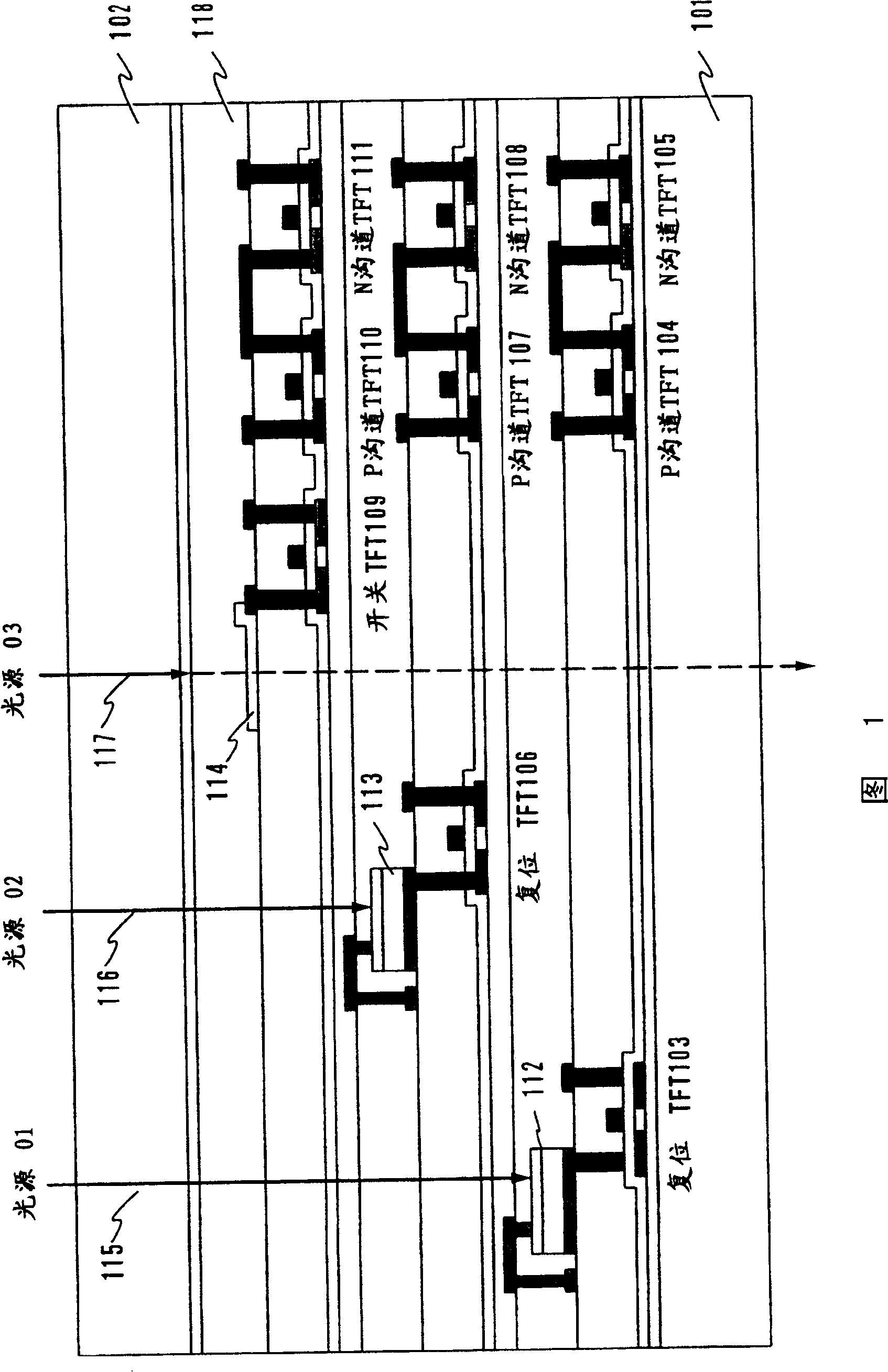
[0076] The light sensor is described in detail below. Figure 4 A circuit diagram of a light sensor portion according to the present invention is shown. In this embodiment, the light sensor consists of a photodiode. Refer below Figure 4 To describe the work of the light sensor part. First, a reset pulse is input into the reset transistor 405 . Here, since a P-channel (hereinafter referred to as Pch) TFT is used as this reset transistor, the signal is low. When the reset transistor 405 is turned on, the cathode potential of the photodiode 401 is raised to the potential level of the power supply. At this time, the storage capacitor of the capacitor 402 is also raised to the potential level of the power supply. When the capacitance of the photodiode 401 is large, the storage capacitor of this capacitor 402 may not be installed intentionally. Next, the reset pulse goes high, and the reset transistor 405 is turned off.
[0077] In the case where no light is input, the cathode...
Embodiment approach 2
[0083] In this embodiment, a liquid crystal is used to form an optical shutter. As is generally known, liquid crystal panels are fabricated by injecting liquid crystal material into liquid crystal gold gaps with a width of a few micrometers, the transmission of light is controlled by an applied voltage, and the liquid crystals are thus used as optical shutters. The entire surface of the substrate does not have to function as a liquid crystal, but since the manufacture of the substrate becomes easier when the liquid crystal is injected over the entire substrate surface in this embodiment, the liquid crystal has been injected. Although the manufacture becomes complicated, it is also possible to employ a structure in which the liquid crystal is cleared from the light input region. In this case, only the portion where the optical shutter exists is surrounded by the sealing material, and the liquid crystal can be injected only into this portion.
[0084] Fig. 8 shows a circuit dia...
Embodiment approach 3
[0090] The various steps according to the present invention are described below with reference to the sectional view of FIG. 10 . In FIG. 10, the optical sensor is composed of TFT and amorphous silicon photodiode, and the optical shutter is composed of liquid crystal. In this embodiment, TFTs and photodiodes are fabricated by the following methods. First, a coating film 1002 is formed on a glass substrate 1001 . An oxide film or a nitride film is formed as this film by a chemical vapor deposition method (hereinafter referred to as CVD method). Next, amorphous silicon is similarly formed into a film by the CVD method. This amorphous silicon film is crystallized by laser annealing method or thermal annealing method. In this way, a polysilicon (p-Si) film can be formed. Next, TFT islands 1003, 1004, 1005 are formed by patterning the polysilicon film. A gate insulator 1006 is then formed by the CVD method.
[0091] Then, as a method for forming the gate electrode, a metal to...
PUM
 Abstract
Description
Claims
Application Information
 - R&D
- Intellectual Property
- Life Sciences
- Materials
- Tech Scout
- Unparalleled Data Quality
- Higher Quality Content
- 60% Fewer Hallucinations
Browse by: Latest US Patents, China's latest patents, Technical Efficacy Thesaurus, Application Domain, Technology Topic, Popular Technical Reports.
© 2025 PatSnap. All rights reserved.Legal|Privacy policy|Modern Slavery Act Transparency Statement|Sitemap|About US| Contact US: help@patsnap.com