Aperiodic capacity loaded phase shifter
A capacitive loading, non-periodic technology, applied to circuits, electrical components, waveguide devices, etc., can solve the problems of increased overall reflection of the phase shifter, increased loss of the phase shifter, etc., to achieve low insertion loss, good impedance matching, Large effect of controllable phase shift
- Summary
- Abstract
- Description
- Claims
- Application Information
AI Technical Summary
Problems solved by technology
Method used
Image


Examples
Embodiment 1
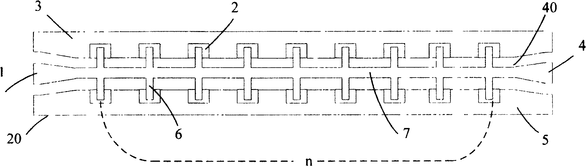
[0025] One of the phase shifters of embodiment 1 aperiodic capacitive loading, its structural schematic diagram is shown in figure 2 .
[0026] In this embodiment, sapphire is used as the substrate 20, and the microwave transmission line 40 is constructed on the substrate 20. The microwave transmission line 40 is a coplanar waveguide transmission line, and the microwave transmission line 40 includes a central signal line 7, a loading capacitor 2, a first grounding line 3, a second The ground wire 5, the input end 1 and the output end 4, the central signal line 7 is located between the first ground wire 3 and the second ground wire 5, and the two ends of the central signal line 7 are respectively the input end 1 and the output end 4, n The loading capacitors 2 with different capacitances are evenly arranged between the central signal line 7 and the grounding lines 3 and 5 of the microwave transmission line 40, and the loading capacitor 2 and the central signal line 7 are conne...
Embodiment 3
[0033] Embodiment 3 The second phase shifter of aperiodic capacitive loading, its structural schematic diagram is shown in image 3 .
[0034] In this embodiment, sapphire is used as the substrate 20, and the microwave transmission line 40 is constructed on the substrate 20. The microwave transmission line 40 is a coplanar waveguide transmission line, and the microwave transmission line 40 includes a central signal line 7, a loading capacitor 2, a first grounding line 3, a second The ground wire 5, the input end 1 and the output end 4, the central signal line 7 is located between the first ground wire 3 and the second ground wire 5, and the two ends of the central signal line 7 are respectively the input end 1 and the output end 4, n Loading capacitors 2 with the same capacitance are unevenly arranged between the central signal line 7 and the first grounding line 3 and the second grounding line 5. As far as the loading position is concerned, its capacitance is an optimized va...
Embodiment 5
[0041] Embodiment 5 The phase shifter with aperiodic capacitive loading is the third.
[0042] In this embodiment, sapphire is used as the substrate 20, and the microwave transmission line 40 is constructed on the substrate 20. The microwave transmission line 40 is a coplanar waveguide transmission line, and the microwave transmission line 40 includes a central signal line 7, a loading capacitor 2, a first grounding line 3, a second The ground wire 5, the input end 1 and the output end 4, the central signal line 7 is located between the first ground wire 3 and the second ground wire 5, and the two ends of the central signal line 7 are respectively the input end 1 and the output end 4, n The loading capacitors 2 with different capacitances are unevenly arranged between the central signal line 7 and the grounding lines 3, 5, and any one of the n loading capacitors 2 is relative to its loading position on the central signal line 7, Its capacitance is an optimized value, and the l...
PUM
 Abstract
Description
Claims
Application Information
 - R&D
- Intellectual Property
- Life Sciences
- Materials
- Tech Scout
- Unparalleled Data Quality
- Higher Quality Content
- 60% Fewer Hallucinations
Browse by: Latest US Patents, China's latest patents, Technical Efficacy Thesaurus, Application Domain, Technology Topic, Popular Technical Reports.
© 2025 PatSnap. All rights reserved.Legal|Privacy policy|Modern Slavery Act Transparency Statement|Sitemap|About US| Contact US: help@patsnap.com