Supercharge Your Innovation With Domain-Expert AI Agents!

Method for improving unevenness of polishing and method for preparing embedded copper metal layer

A copper metal, embedded technology, applied in chemical instruments and methods, semiconductor/solid-state device manufacturing, electrical components, etc., can solve the problems of slow removal of copper oxide layer, inability to be completely removed, prolonged grinding time of semiconductor wafers, etc., to achieve The effect of reducing polishing unevenness, improving product competitiveness, and improving process excellent rate

Inactive Publication Date: 2009-05-06
FUJIAN JINHUA INTEGRATED CIRCUIT CO LTD
View PDF2 Cites 0 Cited by
  • Summary
  • Abstract
  • Description
  • Claims
  • Application Information

AI Technical Summary

Problems solved by technology

Because this method belongs to physical removal, it is not easy to achieve a comprehensive uniformity on the surface of the semiconductor wafer, so it may cause the local copper oxide layer on the semiconductor wafer to be removed too slowly, or even cannot be completely removed, thereby reducing the grinding rate of copper in this area, resulting in Deterioration of with-in-wafer non-uniformity (WIWNU) of semiconductor wafers
[0005] Excessive WIWNU will not only lengthen the grinding time required for semiconductor wafers and reduce productivity, but also increase the over-polish time (over-polish time) will also cause metal dishing on the surface of semiconductor wafers, and even lead to metal dishing. Surface erosion (erosion) and other issues

Method used


Image

  • Method for improving unevenness of polishing and method for preparing embedded copper metal layer
  • Method for improving unevenness of polishing and method for preparing embedded copper metal layer
  • Method for improving unevenness of polishing and method for preparing embedded copper metal layer

Examples


Embodiment Construction

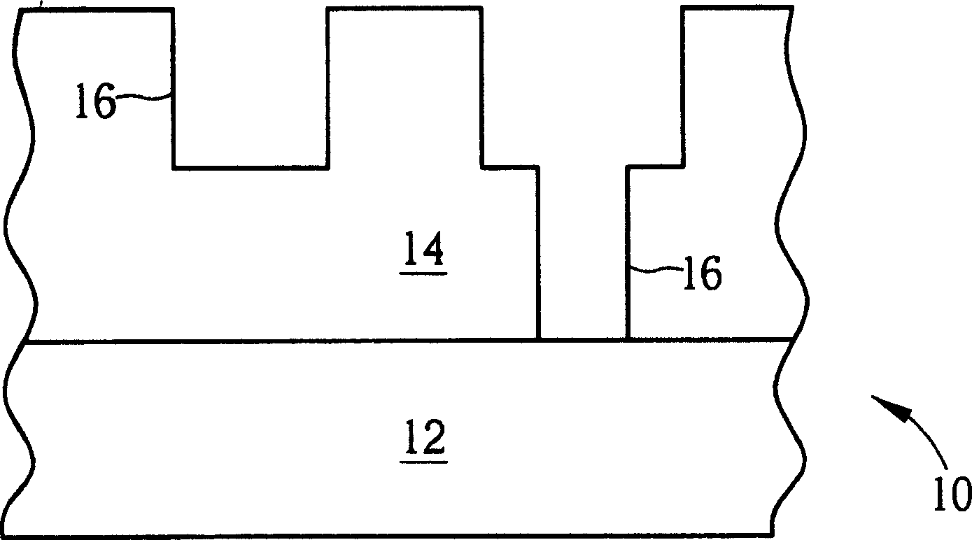
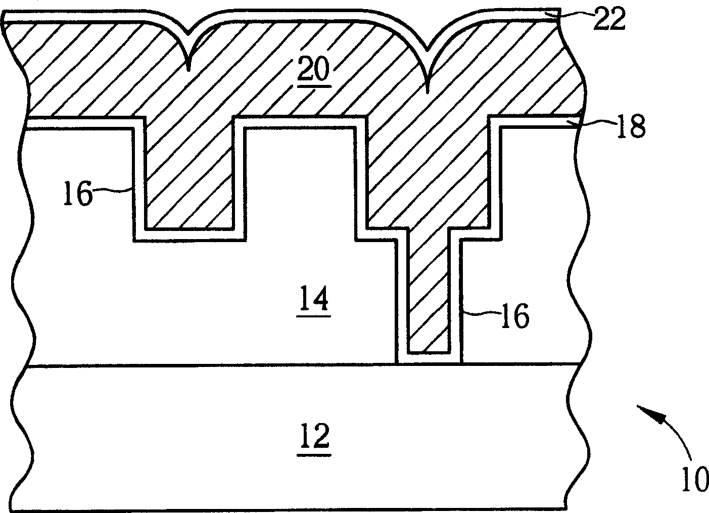
[0017] see Figure 1 to Figure 4 , Figure 1 to Figure 4 It is a schematic diagram of the method for fabricating an embedded copper metal layer on a semiconductor wafer 10 according to the present invention. Such as figure 1 As shown, the semiconductor wafer 10 includes a substrate 12 , a dielectric layer 14 disposed on the surface of the substrate 12 , and a plurality of embedded structures 16 disposed in the dielectric layer 14 . The embedded structure 16 can be designed as a single damascene (single damascene) structure or a dual damascene (dual damascene) structure according to product requirements, and wherein at least one embedded structure 16 penetrates the dielectric layer 14 to be electrically connected downward to the substrate. Conductive regions (not shown) in 12, such as other metal layers or parts of transistors.

[0018] Such as figure 2 As shown, next, a barrier layer 18 is formed on the surface of the semiconductor wafer 10 . The barrier layer 18 uniforml...


PUM


Abstract

First, the invention uses the first chemical solution to clean the surface of copper metal layer, which is formed on the semiconductor wafer. Then, the second chemical solution is utilized to carry out chemico-mechanical polishing in order to remove part of the copper layer. Thus, the remanent copper layer possesses rough flat surface.

Description

technical field [0001] The invention provides a chemical mechanical polishing method, in particular a chemical mechanical polishing method in which a copper metal layer is formed on the surface of a semiconductor wafer. Background technique [0002] In the semiconductor process, the purpose of planarization is to smooth the undulating surface of the semiconductor wafer, so as to improve the accuracy of subsequent pattern transfer. Chemical-mechanical polishing (CMP) is almost the only planarization process that can provide global planarization. The principle is to place the semiconductor wafer on a polishing table, cooperate with appropriate chemical reagents (reagent) and abrasive particles, and use chemical reaction and mechanical grinding at the same time to remove the uneven contour of the surface of the semiconductor wafer. To be smoothed. [0003] The chemical mechanical polishing method is widely used, especially in the copper wire process, it is one of the key tech...

Claims


Application Information

Patent Timeline
Patent Type & Authority Patents(China)
IPC IPC(8): H01L21/302H01L21/3213C09K3/14C23F1/00H01L21/768
Inventor 胡绍中许嘉麟蔡腾群余志展
Owner FUJIAN JINHUA INTEGRATED CIRCUIT CO LTD
Features
  • R&D
  • Intellectual Property
  • Life Sciences
  • Materials
  • Tech Scout
  • Unparalleled Data Quality
  • Higher Quality Content
  • 60% Fewer Hallucinations
Learn More