Supercharge Your Innovation With Domain-Expert AI Agents!

Liquid crystal display board

A technology for liquid crystal display panels and substrates, which is applied to optics, instruments, electrical components, etc., can solve the problem of the limitation of the display aperture ratio of the pixel structure 100, and achieve the effect of high aperture ratio and wide viewing angle aperture ratio.

Active Publication Date: 2009-07-29
AU OPTRONICS CORP
View PDF7 Cites 0 Cited by
  • Summary
  • Abstract
  • Description
  • Claims
  • Application Information

AI Technical Summary

Problems solved by technology

However, such a design limits the display aperture ratio of the pixel structure 100

Method used


Image

  • Liquid crystal display board
  • Liquid crystal display board
  • Liquid crystal display board

Examples


Embodiment Construction

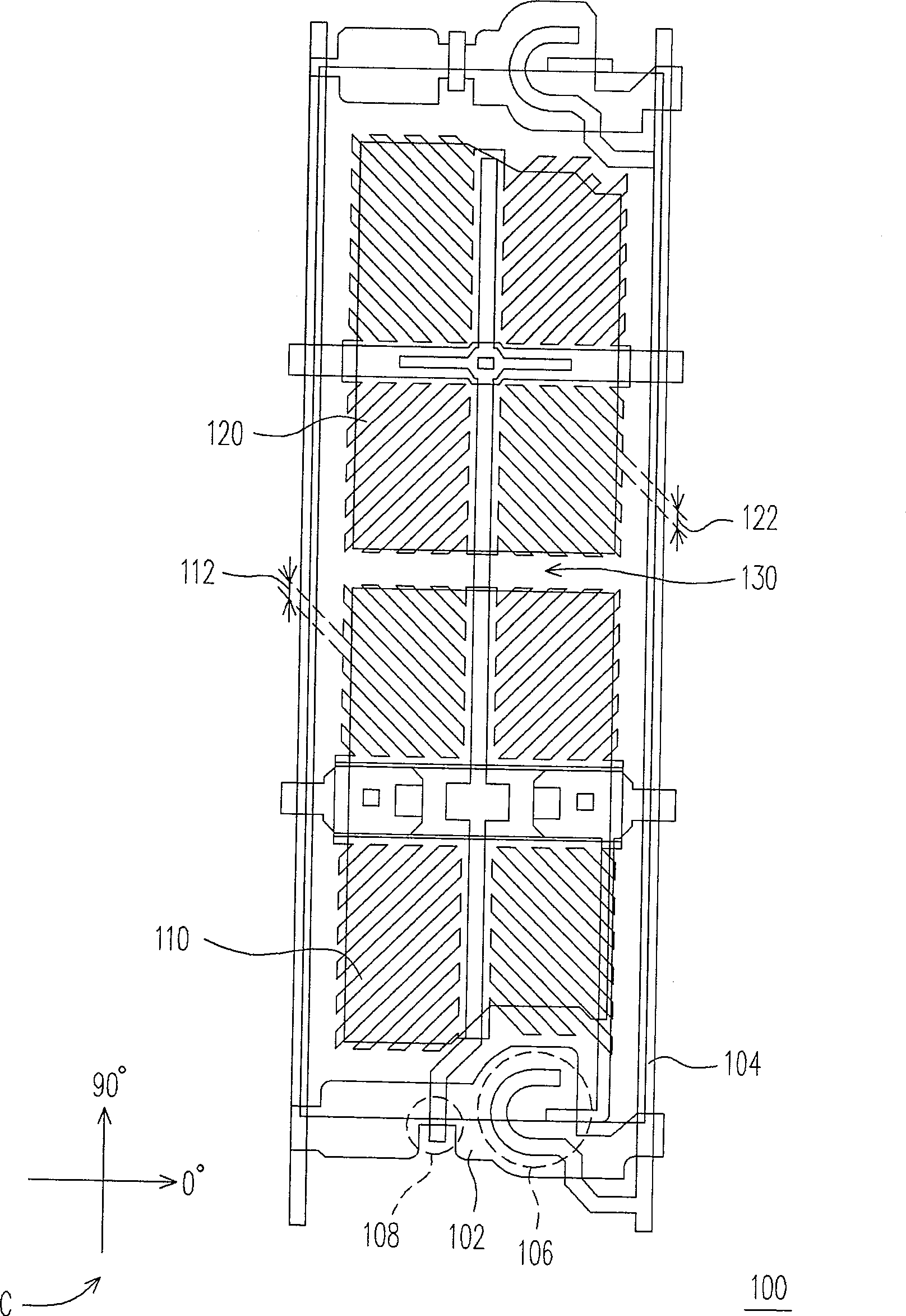
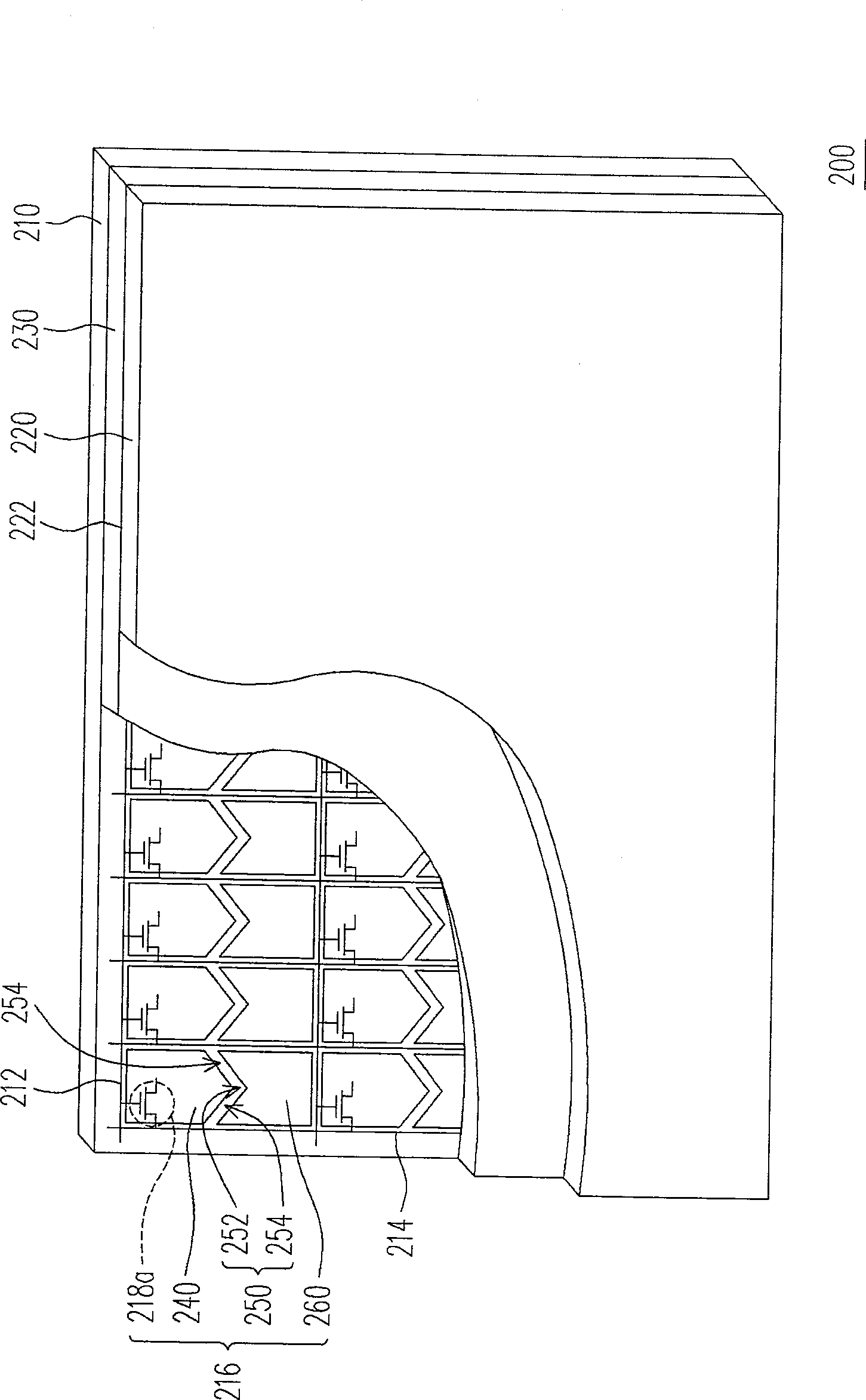
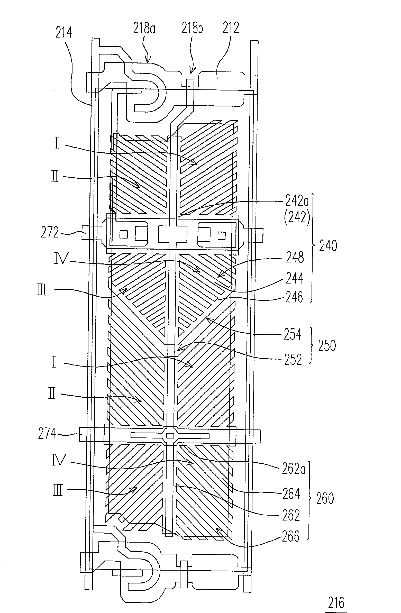
[0066] Figure 2A It is a schematic top view of a polymer stabilized alignment liquid crystal display panel (Polymer Stabilized Alignment Liquid Crystal Display Panel, PSA-LCD) according to the first embodiment of the present invention, and Figure 2B shown as Figure 2A The pixel structure of the liquid crystal display panel. Please refer to Figure 2A The liquid crystal display panel 200 includes a first substrate 210 , a plurality of scan lines 212 , a plurality of data lines 214 , a plurality of pixel structures 216 , a second substrate 220 and a liquid crystal layer 230 . The scan lines 212 , the data lines 214 and the pixel structures 216 are all disposed on the first substrate 210 . The pixel structure 216 is electrically connected to the corresponding scan line 212 and the data line 214 . The liquid crystal layer 230 is disposed between the first substrate 210 and the second substrate 220 .

[0067] Each pixel structure 216 includes a first active element 218 a , ...


PUM

PropertyMeasurementUnit
widthaaaaaaaaaa

Abstract

A liquid crystal display panel includes a first substrate, a plurality of scanning lines, a plurality of data lines, a plurality of pixel structures, a second substrate and a liquid crystal layer. The scan lines, the data lines and the pixel structures are all disposed on the first substrate. The pixel structures are electrically connected with the corresponding scan lines and data lines. The liquid crystal layer is disposed between the first substrate and the second substrate. Each pixel structure includes a first active element, a first pixel electrode, and a second pixel electrode. The first pixel electrode is electrically connected to the first active element. A V-shaped main slit is formed between the first pixel electrode and the second pixel electrode. The V-shaped main slit has a tip and two branches connected to the tip, wherein the tip faces the second pixel electrode, and the edge of the first pixel electrode adjacent to each branch is substantially parallel to the edge of the second pixel electrode. In the present invention, the liquid crystal molecules located above the V-shaped main slits are tilted in an appropriate direction. The liquid crystal display panel of the present invention can have both wide viewing angle and high aperture ratio display effect.

Description

technical field [0001] The present invention relates to a display panel, and in particular to a liquid crystal display panel. Background technique [0002] In the market, the display viewing angle range of liquid crystal displays is increasingly required. Currently, a common wide viewing angle technology is a multi-domain vertical alignment liquid crystal display panel, which uses an alignment structure to make liquid crystal molecules in different regions tilt in different directions to achieve a wide viewing angle effect. However, the disclination of the liquid crystal molecules around the alignment structure is often unclear, which may cause light leakage. Therefore, an alignment method using polymer-stablized alignment (PSA) with pixel electrodes with multiple micro-slits to form multi-domain alignment was proposed to improve multi-domain vertical alignment. The problem of poor display effect of the LCD panel. [0003] figure 1 It is a well-known pixel structure of a...

Claims


Application Information

Patent Timeline
Patent Type & Authority Patents(China)
IPC IPC(8): G02F1/1362G02F1/1343H01L27/12
Inventor 陈介伟詹德威苏振嘉
Owner AU OPTRONICS CORP
Features
  • R&D
  • Intellectual Property
  • Life Sciences
  • Materials
  • Tech Scout
  • Unparalleled Data Quality
  • Higher Quality Content
  • 60% Fewer Hallucinations
Learn More