Check patentability & draft patents in minutes with Patsnap Eureka AI!

Luminous diode structure and its manufacture method

A technology of light-emitting diodes and manufacturing methods, which is applied to electrical components, circuits, semiconductor devices, etc., and can solve problems such as quantum well crystal defects, InGaN and GaN lattice mismatch, affecting device light extraction efficiency and luminous intensity, etc., to achieve ease of use , Improve the light extraction efficiency and luminous intensity, and improve the crystal quality

Active Publication Date: 2009-11-11
EPILIGHT TECH
View PDF1 Cites 0 Cited by
  • Summary
  • Abstract
  • Description
  • Claims
  • Application Information

AI Technical Summary

Problems solved by technology

[0003] The N-type GaN layer of the existing light-emitting diode is directly above the multi-quantum well layer. However, due to the lattice mismatch between InGaN and GaN, there will be defects in the crystal of the quantum well, which will affect the light extraction efficiency and luminous intensity of the device.

Method used


Image

  • Luminous diode structure and its manufacture method
  • Luminous diode structure and its manufacture method
  • Luminous diode structure and its manufacture method

Examples


Embodiment Construction

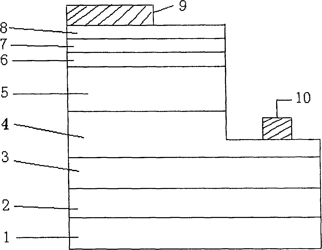
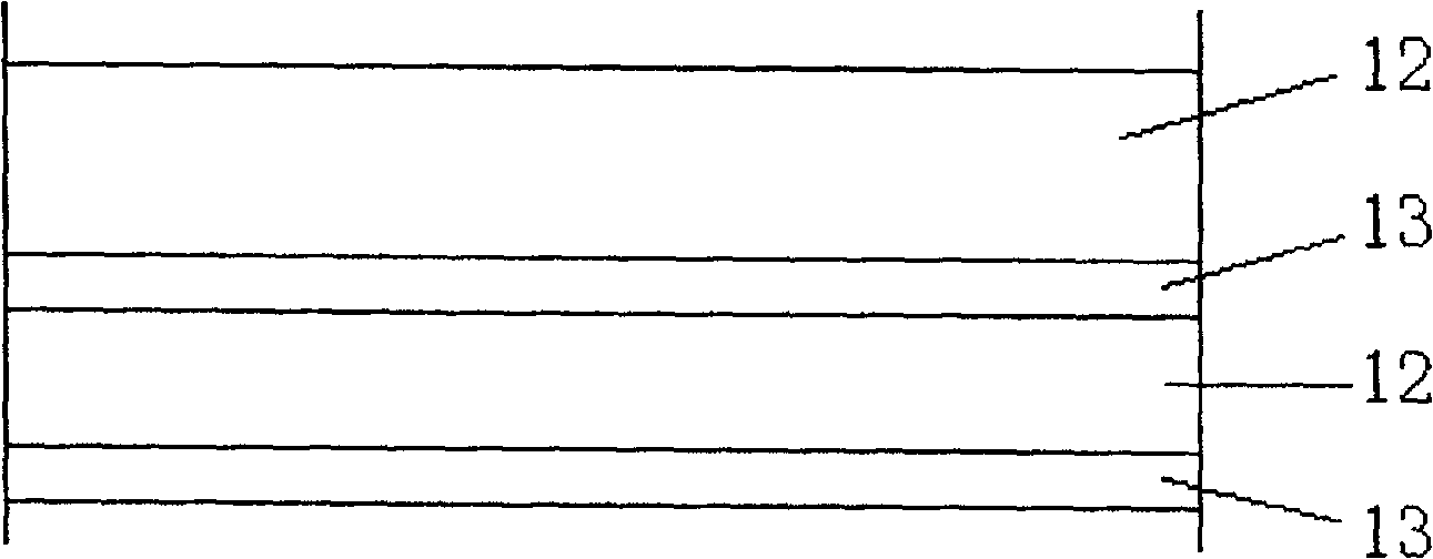
[0017] The structure of light-emitting diode of the present invention can refer to figure 2 As shown, it includes substrate layer 1, buffer layer 2, undoped GaN layer 3, N-type GaN layer 4, multiple quantum well layer 5, P-type AlGaN layer 6, P-type GaN layer 7 and contacts from bottom to top. Layer 8, a P-type electrode is arranged on the contact layer, and an N-type electrode is arranged on the N-type GaN layer. The N-type GaN layer is doped with Si element. There is also a multi-quantum well buffer layer 11 between the N-type GaN layer 4 and the multi-quantum well layer 5, and the multi-quantum well buffer layer 11 includes one or more composite structures of InGaN / GaN, each The composite structure of InGaN / GaN all includes a layer of InGaN layer 12 located below and a layer of GaN layer 13 located above. In the composite structure of InGaN / GaN, the thickness of the InGaN layer 12 is greater than that of the GaN layer 13. thickness, the InGaN layer 12 has a lower In dopi...


PUM


Abstract

The invention discloses a light-emitting diode structure, which includes an N-type GaN layer, a multi-quantum well layer, and a P-type AlGaN layer, and a multi-quantum well buffer layer is separated between the N-type GaN and the multi-quantum well layer , the multi-quantum well buffer layer includes one or more composite structures of InGaN / GaN, the thickness of the InGaN layer in the composite structure of InGaN / GaN is 60~500, and the thickness of the GaN layer is 10~50 . The invention also discloses a method for fabricating the structure of the light-emitting diode, which includes alternately growing InGaN layers and GaN layers to form a multi-quantum well buffer layer with a composite structure. In the present invention, the light-emitting diode structure with multiple quantum well buffer layers is produced through simple steps through the above-mentioned method, which is very easy to use, and the crystal quality of the light-emitting diode produced is improved, thereby improving the light extraction efficiency and luminescence of the light-emitting diode strength.

Description

technical field [0001] The invention relates to a structure of a light emitting diode. The invention also relates to a method for manufacturing the structure of the light emitting diode. Background technique [0002] The structure of existing light-emitting diodes can be found in figure 1 As shown, it includes substrate layer 1, buffer layer 2, undoped GaN layer 3, N-type GaN layer 4, multiple quantum well layer 5, P-type AlGaN layer 6, P-type GaN layer 7 and contacts from bottom to top. Layer 8, a P-type electrode is arranged on the contact layer, and an N-type electrode is arranged on the N-type GaN layer. The N-type GaN layer is doped with Si element. Use MOCVD (MetalOrganic Chemical Vapor Deposition) to grow GaN light-emitting diodes, using Al 2 o 3 As the substrate layer 1, a buffer layer 2 is grown next. The growth temperature of the buffer layer 2 is 530°C, and its thickness is The growth temperature of the undoped GaN layer 3 is 1050° C., and the thickness is ...

Claims


Application Information

Patent Timeline
Patent Type & Authority Patents(China)
IPC IPC(8): H01L33/00
Inventor 林振贤郑文荣
Owner EPILIGHT TECH
Features
  • R&D
  • Intellectual Property
  • Life Sciences
  • Materials
  • Tech Scout
  • Unparalleled Data Quality
  • Higher Quality Content
  • 60% Fewer Hallucinations
Learn More