Supercharge Your Innovation With Domain-Expert AI Agents!

Printed circuit board assembly and method of producing the same

A technology for printed circuit boards and components, which is used in printed circuit manufacturing, printed circuit components, printed circuits, etc., and can solve problems such as chipping and leakage of electroplating layers

Inactive Publication Date: 2010-01-13
YAZAKI CORP
View PDF8 Cites 1 Cited by
  • Summary
  • Abstract
  • Description
  • Claims
  • Application Information

AI Technical Summary

Problems solved by technology

[0006] However, in crimp connection, when the terminal is pressed into the through hole, the plating layer formed on the surface of the terminal is scratched and chips are generated
This shavings may adhere to other conductive parts, causing leakage

Method used


Image

  • Printed circuit board assembly and method of producing the same
  • Printed circuit board assembly and method of producing the same
  • Printed circuit board assembly and method of producing the same

Examples


Embodiment Construction

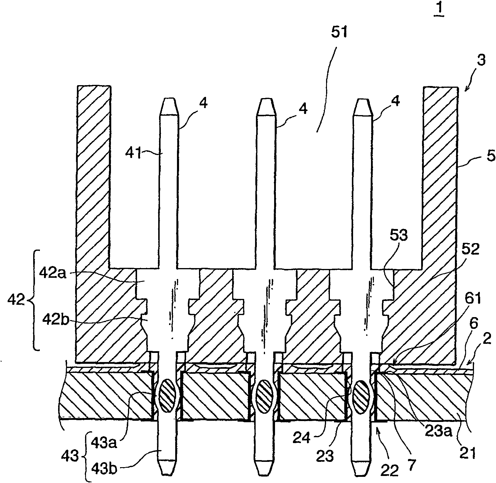
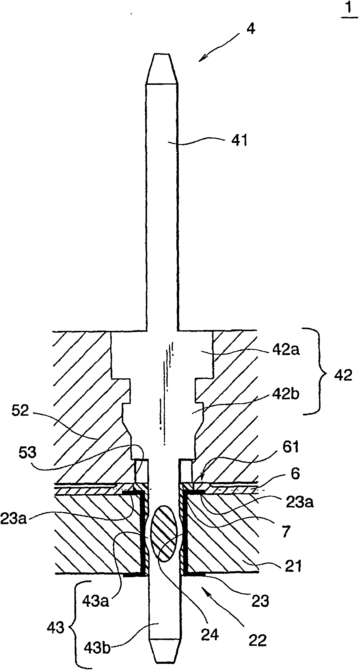
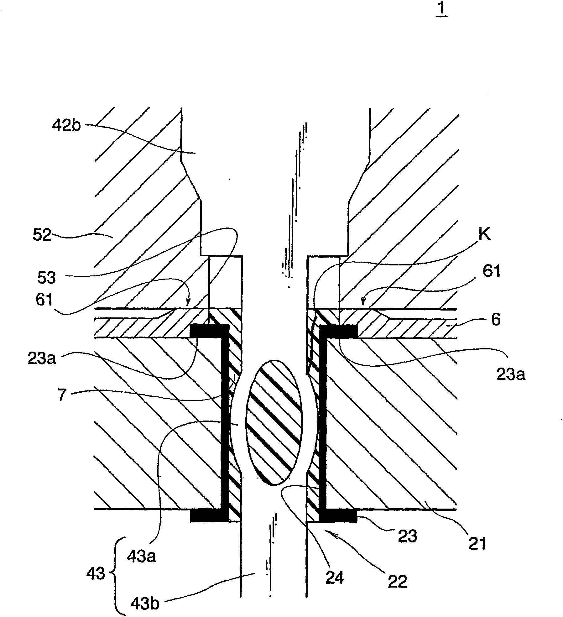
[0034] will refer to Figures 1 to 7 A printed circuit board assembly 1 according to a first embodiment of the present invention is explained.

[0035] Such as figure 1 As shown, a printed circuit board assembly 1 is formed by attaching a crimp connector 3 to a printed circuit board 2 . The printed circuit board 2 includes an insulating plate 21 made of insulating synthetic resin, a conductive pattern (not shown) wired in a predetermined pattern on the insulating plate 21, a through-hole portion 22 electrically connected to the conductive pattern, 21 on the protective layer 6, and the overlapping protective layer portion 61.

[0036] The through-hole portion 22 includes a through-hole 24 penetrating the insulating board 21 , a metal plating portion 23 formed on the inner side of the through-hole 24 , and an outer periphery of the through-hole 24 provided on the surface of the insulating board 21 . Further, the lead-out portion 23a of the metal plating portion 23 is a portio...


PUM


Abstract

A printed circuit board assembly is formed by a press-fit connector attached to a printed circuit board. The press-fit connector includes a plurality of press-fit terminals and a housing. An overlapping resist part is formed on the printed circuit board. The overlapping resist part closely contacts the housing, and is arranged in a circular shape at an outer circumference of a through hole. By dipping the housing and the overlapping resist part closely contacting each other into a synthetic resin bath, the synthetic resin is filled in an inside of the through hole and a space surrounded by the overlapping resist part, and swarf of the press-fit terminal is fixed in the synthetic resin.

Description

[0001] Cross References to Related Applications [0002] This application is based on Japanese Patent Application No. 2006-137359, the contents of which are hereby incorporated by reference. technical field [0003] The present invention relates to a printed circuit board assembly comprising a printed circuit board having a crimp connector, and to a method of manufacturing the same, in particular for preventing the The crimp connector terminal swarf produced when the through-hole is stuck to other conductors of the printed circuit board assembly. Background technique [0004] Conventionally, when an electrical component having a pin-shaped terminal is mounted on a printed circuit board, for example, the terminal is inserted through a hole in the printed circuit board, and is brazed to close the hole, The terminals are thereby electrically connected to conductive patterns formed on the surface of the printed circuit board. On the other hand, recently, instead of the solder ...

Claims


Application Information

Patent Timeline
Patent Type & Authority Patents(China)
IPC IPC(8): H05K1/18H05K1/02H05K3/32H01R13/52
CPCH01R12/7064H05K2203/1361H05K2201/0959H05K2201/10189H01R13/5216H05K2201/10977H01R12/585H05K3/308H05K3/284H05K2201/1059Y10T29/49153
Inventor 松村薰
Owner YAZAKI CORP
Features
  • R&D
  • Intellectual Property
  • Life Sciences
  • Materials
  • Tech Scout
  • Unparalleled Data Quality
  • Higher Quality Content
  • 60% Fewer Hallucinations
Learn More