

Memory array circuit
A memory array and circuit technology, applied in static memory, read-only memory, digital memory information, etc., can solve problems such as inability to store components, achieve high-speed reading work, and reduce parasitic capacitance.
- Summary
- Abstract
- Description
- Claims
- Application Information
AI Technical Summary
Problems solved by technology
Method used
Image


Examples
Embodiment 1
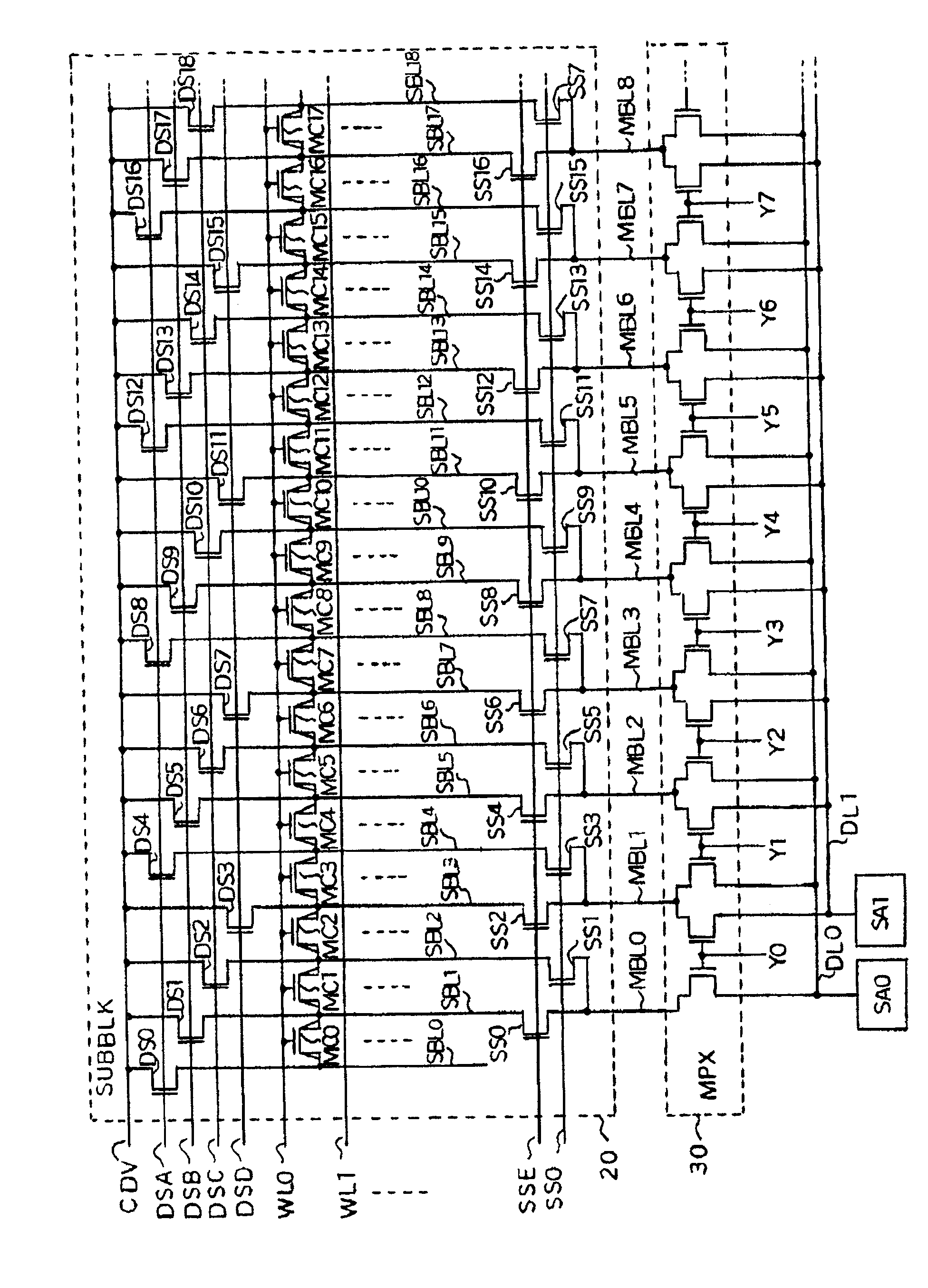
[0042] figure 1 is a configuration diagram showing a memory array circuit according to Embodiment 1 of the present invention.
[0043] This memory array circuit has a plurality of subblocks (SUBBLK) 20 (only one of which is shown in the figure) and one multiplexer (MPX) 30 . Each sub-block 20 has a plurality of word lines WLi (i=0, 1, . . . ) arranged in parallel and a plurality of sub bit lines SBLj (j=0, 1, .. .).
[0044] Memory cells MCj (j=0, 1, . . . ) are provided at intersections of word line WLi and sub bit line SBLj (only memory cells corresponding to word line WL0 are shown in the figure). like Figure 4 As shown, each memory cell MCj is a nonvolatile memory element corresponding to 2 bits as follows: memory function bodies are respectively formed on the left and right sidewalls of the gate electrode (control electrode), and memory function bodies are formed corresponding to the two memory function bodies. The left and right diffusion regions are made into the ...
Embodiment 2
[0060] Figure 7 It is a configuration diagram showing a memory array circuit according to Embodiment 2 of the present invention.
[0061] and figure 1 Similarly, the memory array circuit has a plurality of sub-blocks 20A and one multiplexer 30 . Each sub-block 20A has a plurality of word lines WLi (i=0, 1, . . . ) arranged in parallel and a plurality of sub bit lines SBLj (j=0, 1, .. .). Furthermore, at each intersection of the word line WLi and the sub bit line SBLj, a figure 1 For the same memory cell MCj, the gate electrode of the memory cell MCj is connected to the bit line WLi. The first and second electrodes of memory cell MCj are connected to sub bit lines SBLj and SBLj+1, respectively. Furthermore, one end of sub bit line SBLj is connected to common power supply line CDV via drain selector DSj. previous structure and figure 1 The memory array circuit is the same.
[0062] On the other hand, the gates of the 6nth (where n=0, 1, 2, . . . ) drain selectors amo...
Embodiment 3
[0072] Figure 8 is a configuration diagram showing a memory array circuit according to Embodiment 3 of the present invention.
[0073] and figure 1 Similarly, the memory array circuit has a plurality of sub-blocks 20B and one multiplexer 30 . Each sub-block 20B has a plurality of word lines WLi (i=0, 1, . j = 0, 1, . . . ). Furthermore, at each intersection of the word line WLi and the sub bit line SBLj, a figure 1 For the same memory cell MCj, the gate of the memory cell MCj is connected to the word line WLi. The first and second electrodes of memory cell MCj are connected to sub bit lines SBLj and SBLj+1, respectively. One end of sub bit line SBLj is connected to common power supply line CDV via drain selector DSj. previous structure with figure 1 The memory array circuit is the same.
[0074] On the other hand, the gates of the 8nth (where n=0, 1, 2, . . . ) drain selectors among the drain selectors DSj are commonly connected to the drain select line DSA. Simil...
PUM
 Abstract
Description
Claims
Application Information