Supercharge Your Innovation With Domain-Expert AI Agents!

Making method of CMOS part

An oxide semiconductor and complementary metal technology, which is applied in semiconductor/solid-state device manufacturing, electrical components, circuits, etc., can solve the problems of increasing photolithography steps, increasing costs, and increasing process complexity, so as to eliminate the need for photolithography processes, The effect of cost saving and cost reduction

Active Publication Date: 2008-01-16
SEMICON MFG INT (SHANGHAI) CORP +1
View PDF1 Cites 5 Cited by
  • Summary
  • Abstract
  • Description
  • Claims
  • Application Information

AI Technical Summary

Problems solved by technology

[0003] In the manufacture of complementary metal oxide transistors in the prior art, when adjusting the threshold voltage, it is first necessary to define the P-well area by photolithography to pre-dope the P-well, then remove the photoresist, and then perform simultaneous N-well Doping with P-well increases additional photolithography steps, and the semiconductor body substrate needs to enter the ion implantation equipment twice, which increases the complexity of the process, prolongs the product production cycle and increases the cost

Method used


Image

  • Making method of CMOS part
  • Making method of CMOS part
  • Making method of CMOS part

Examples


Embodiment Construction

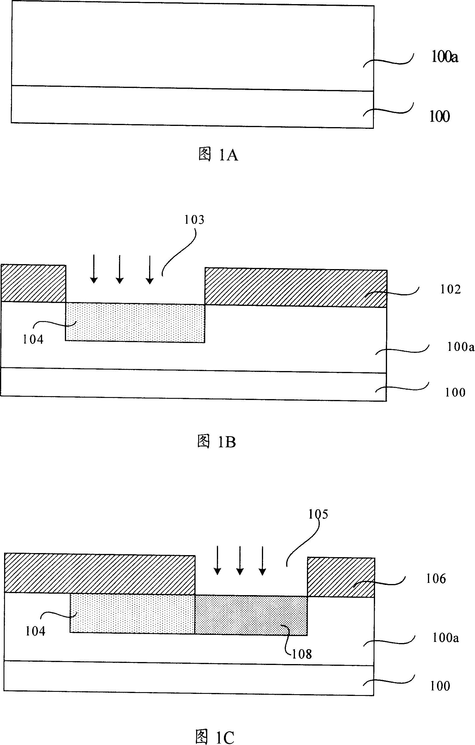
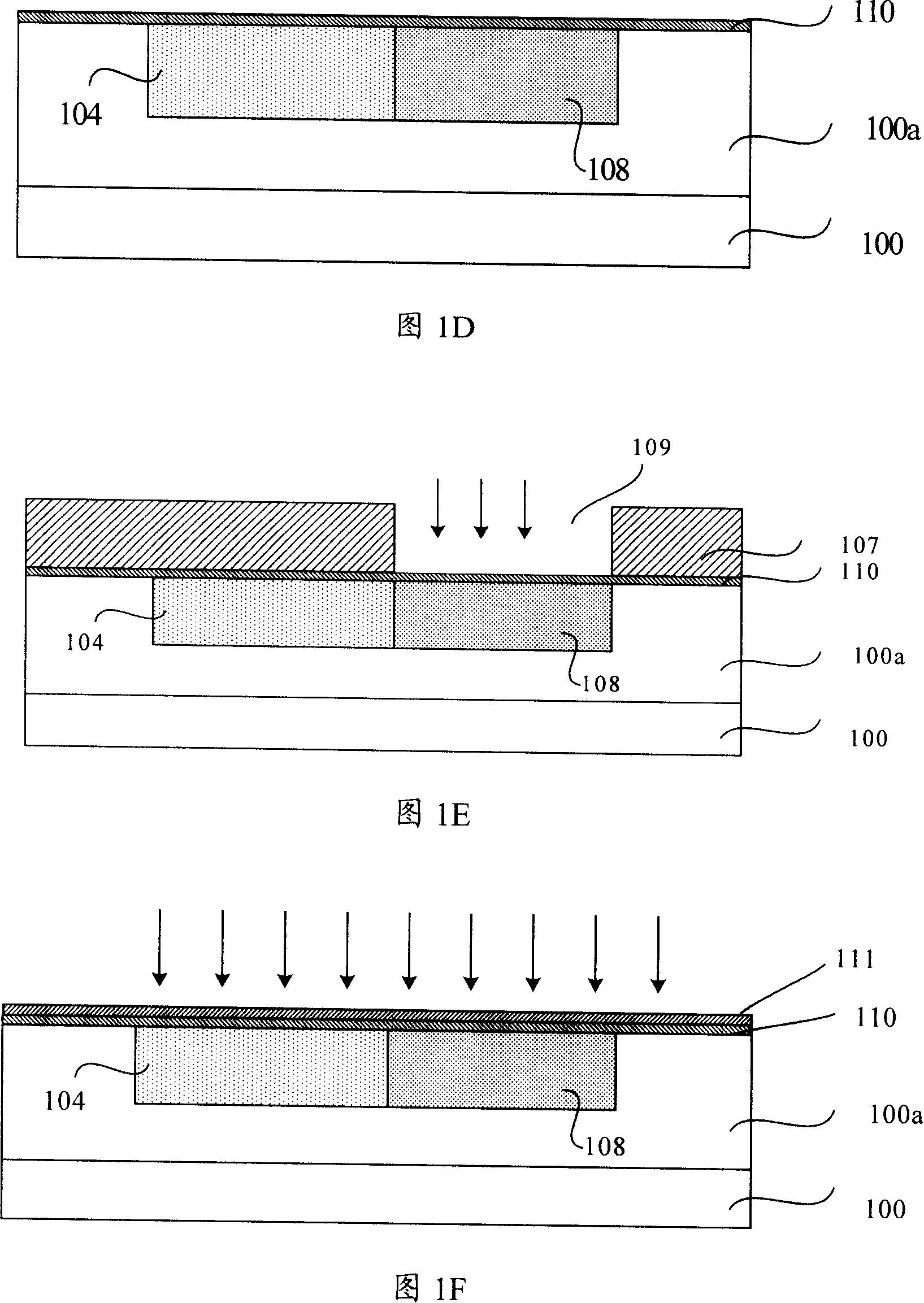
[0075] The specific embodiments of the present invention will be described in detail below in conjunction with the accompanying drawings.

[0076] In the manufacturing process of the complementary metal oxide semiconductor device of the present invention, a semiconductor substrate is provided and after the conductive channel region for manufacturing NMOS and PMOS is formed, the semiconductor substrate is sent into the ion implantation equipment to perform the first stage and The ion implantation doping in the second stage realizes the adjustment of the threshold voltage of NMOS and PMOS, and then manufactures the gate, source, drain and interconnection lines.

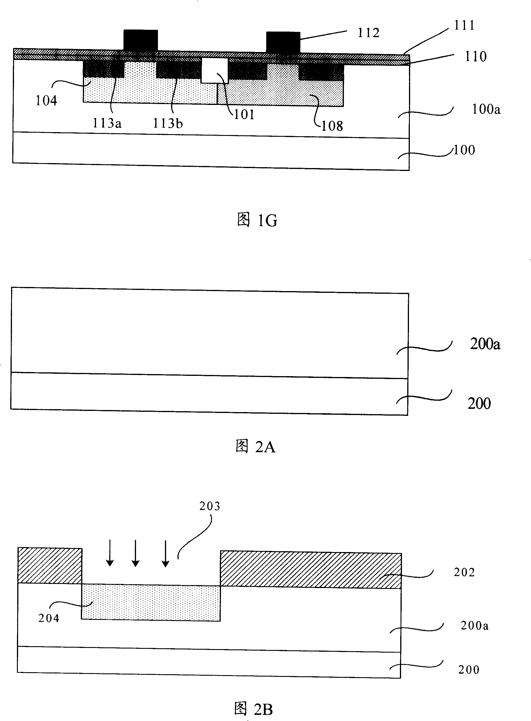
[0077] 2A to 2F are schematic cross-sectional views of the first embodiment of the method of the present invention.

[0078] As shown in FIG. 2A , a semiconductor substrate 200 is provided, and the substrate can be a P-type or an N-type substrate. An epitaxial layer 200a is formed on the substrate. The epitaxial layer...


PUM


Abstract

A method for fabricating a complementary metal oxide semiconductor device includes that a semiconductor substrate is provided; N wells and P wells are formed on the semiconductor substrate; an oxide layer is formed on the semiconductor substrate; the N wells and the P wells are doped in the first stage; the N wells and the P wells are doped in the second stage; in the region of N wells and P wells, a gate cathode, a source cathode, a drain cathode and a interconnection layer are formed. With the invention utilizing different energies, the trenched regions are successively doped to change the threshold voltage, reducing the technique processes, saving the cost and shortening the fabrication cycle.

Description

technical field [0001] The invention relates to the technical field of semiconductor manufacturing, in particular to a manufacturing method of a complementary metal oxide semiconductor device. Background technique [0002] Complementary metal oxide semiconductor devices are widely used in computer and communication fields due to their low voltage, low power consumption, and high integration. Chinese patent application number 200510069668.2 discloses a complementary metal oxide semiconductor device and a manufacturing method thereof. Complementary metal oxide semiconductor devices integrate N-type metal oxide semiconductor transistors (NMOS) and P-type metal oxide semiconductor transistors (PMOS) on the same integrated circuit. Due to the different working modes of NMOS and PMOS, the threshold voltage adjustment need to be done separately. 1A to 1F are the manufacturing methods of complementary metal oxides in the prior art. As shown in FIG. 1A , firstly, a P-type semicond...

Claims


Application Information

Patent Timeline
Patent Type & Authority Applications(China)
IPC IPC(8): H01L21/8238
Inventor 杨勇胜邢溯肖德元
Owner SEMICON MFG INT (SHANGHAI) CORP
Features
  • R&D
  • Intellectual Property
  • Life Sciences
  • Materials
  • Tech Scout
  • Unparalleled Data Quality
  • Higher Quality Content
  • 60% Fewer Hallucinations
Learn More