
Method and structure for reducing floating body effects in mosfet devices

A device and active device technology, applied in the field of semiconductor device processing, can solve problems such as low speed, reduced switching current, and increased thermal power

Inactive Publication Date: 2008-05-21
格芯公司
View PDF0 Cites 6 Cited by
  • Summary
  • Abstract
  • Description
  • Claims
  • Application Information

AI Technical Summary

Problems solved by technology

Unfortunately, as opposed to source diode leakage in switching devices, drain diode leakage increases the thermal power dissipated in the circuit and reduces the actual switching current, resulting in lower speed

Method used


Image

  • Method and structure for reducing floating body effects in mosfet devices
  • Method and structure for reducing floating body effects in mosfet devices
  • Method and structure for reducing floating body effects in mosfet devices

Examples


Embodiment Construction

[0014] Disclosed herein is a method and structure for reducing floating body effects in MOSFET devices, including silicon-on-insulator (SOI) type devices, without junction leakage. Briefly stated, embodiments disclosed herein provide a metal plug formed through the source region of a transistor device such that the plug extends into the body of the transistor and provides a short circuit between the source and the bulk.

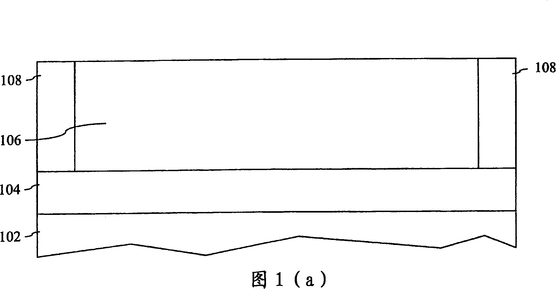
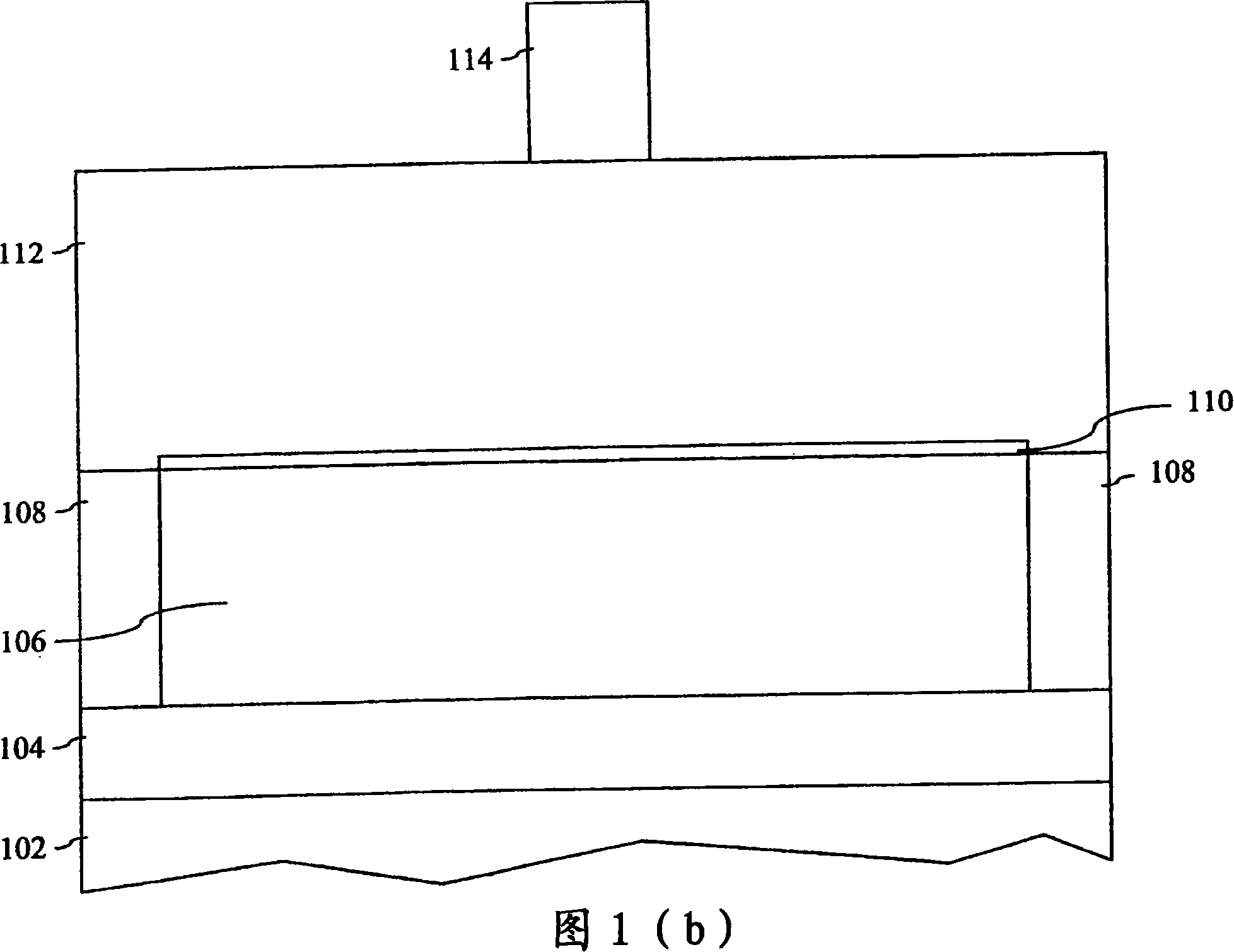
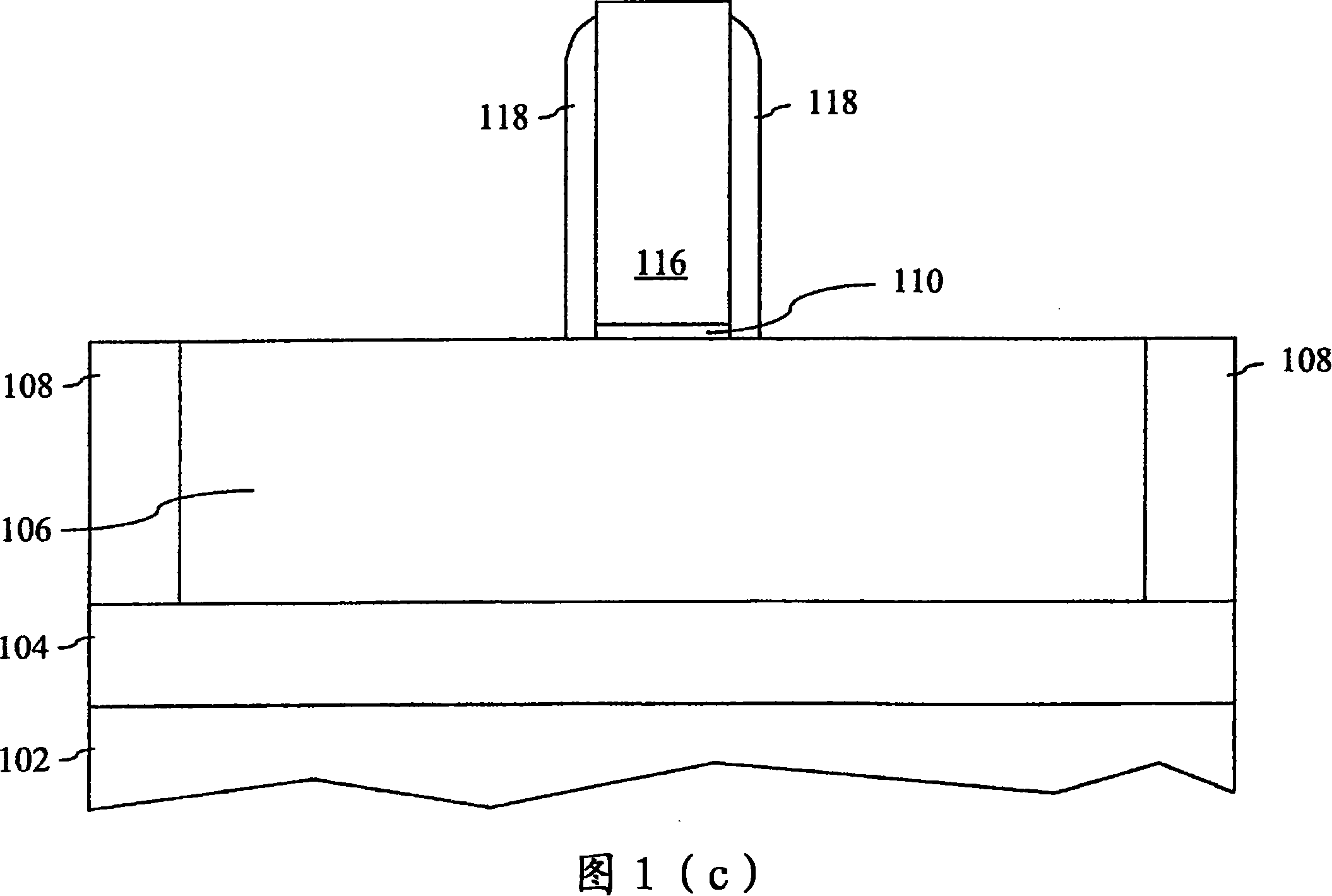
[0015] Reference is initially made to FIGS. 1( a ) through 1 ( k ), which illustrate a series of methods and structures for reducing floating body effects in silicon-on-insulator (SOI) transistor devices according to embodiments of the present invention. Section view. As shown in FIG. 1( a ), a bulk silicon layer 102 has a buried insulator (eg, oxide) layer (BOX) 104 formed thereon. A layer of crystalline silicon 106 is then formed over the BOX layer 104; thus, the term silicon-on-insulator (SOI) is also used to describe layer 106 in which active transistor ...


PUM


Abstract

A field effect transistor (FET) device includes a body substrate, a gate insulating layer formed over the body substrate, a source formed in an active device region associated with the body substrate, and a gate insulating layer formed over the body substrate. a drain region, each of said source and drain regions defining a p / n junction with respect to a body region of said active device region, and a junction formed within a cavity defined in said source region across said The p / n junction of the source region and into a conductive plug in the body region, wherein the conductive plug facilitates a discharge path between the body region and the source region.

Description

technical field [0001] The present invention relates generally to semiconductor device processing techniques and, more particularly, to a method and structure for reducing floating body effects in metal oxide semiconductor field effect transistor (MOSFET) devices, including silicon-on-insulator (SOI) devices . Background technique [0002] Demands for increased performance, functionality, and manufacturing economics of integrated circuits have led to enormous integration densities in order to reduce signal propagation times and increase noise immunity, while also increasing the number of chips that can be formed on a chip or wafer by a single process sequence. Number of circuits and components. Scaling devices to such small dimensions limits operating margins and necessitates increased uniformity in the electrical characteristics of semiconductor devices formed on a chip. [0003] To meet the latter criteria, silicon-on-insulator (SOI) wafers are used to take advantage of ...

Claims


Application Information

Patent Timeline
IPC IPC(8): H01L29/78H01L29/786H01L21/336
CPCH01L29/66636H01L21/743H01L21/26506H01L29/41766H01L29/7833H01L29/78684H01L29/6656H01L29/665H01L29/78612H01L29/0847
Inventor 朱慧珑梁擎擎
Owner 格芯公司
Learn More