CMOS structure and its making method
一种衬底、器件的技术,应用在CMOS结构领域,能够解决难不同应力和应变水平等问题
- Summary
- Abstract
- Description
- Claims
- Application Information
AI Technical Summary
Problems solved by technology
Method used
Image

Examples
Embodiment Construction
[0014] The present invention is understood from the following description and includes CMOS structures that include different channel material compositions within the CMOS structure between the n-FET device channel and the p-FET Different levels of mechanical stress and strain are provided in the device channel. The following description is to be understood within the scope of the above-mentioned figures. Since the drawings are intended for illustrative purposes, they are not necessarily drawn to scale.
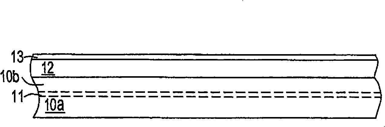
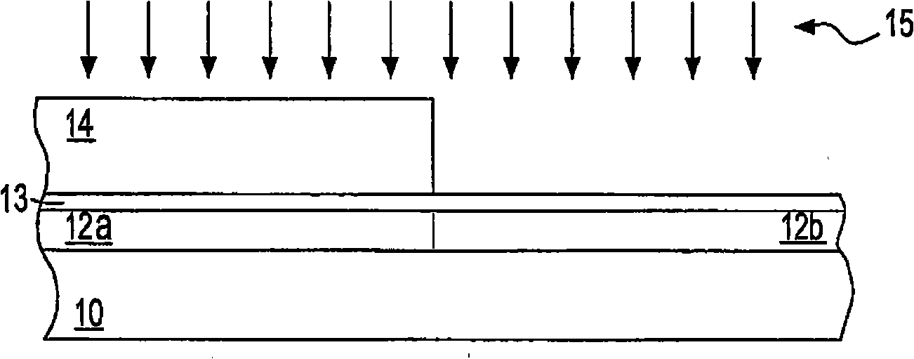
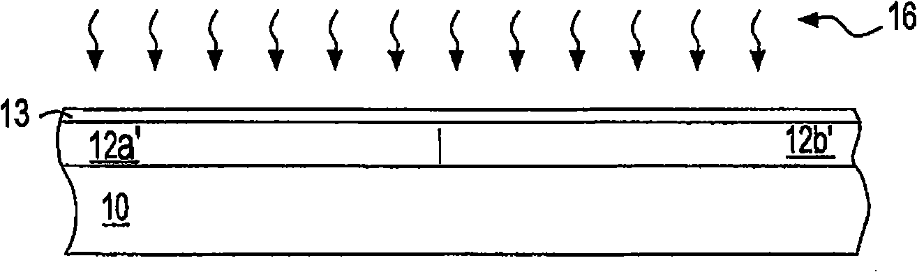
[0015] Figure 1 to Figure 14 A series of schematic cross-sectional views are shown illustrating the results of progressive stages in the fabrication of a CMOS structure according to certain embodiments of the invention. Particular embodiments of the invention include preferred embodiments of the invention. figure 1 A schematic cross-sectional view of a CMOS structure according to a preferred embodiment is shown at an initial stage of fabrication.
[0016] figure 1 A ba...
PUM
 Abstract
Description
Claims
Application Information
 - R&D
- Intellectual Property
- Life Sciences
- Materials
- Tech Scout
- Unparalleled Data Quality
- Higher Quality Content
- 60% Fewer Hallucinations
Browse by: Latest US Patents, China's latest patents, Technical Efficacy Thesaurus, Application Domain, Technology Topic, Popular Technical Reports.
© 2025 PatSnap. All rights reserved.Legal|Privacy policy|Modern Slavery Act Transparency Statement|Sitemap|About US| Contact US: help@patsnap.com