Method and apparatus for measuring wafer surface flatness
A technology of surface flatness and measurement method, which is applied in measurement devices, optical devices, photolithographic process exposure devices, etc., can solve problems such as complicated calculation methods, and achieve the effect of simple operation and easy implementation.
- Summary
- Abstract
- Description
- Claims
- Application Information
AI Technical Summary
Problems solved by technology
Method used
Image


Examples
Example Embodiment
[0018] The specific embodiments of the present invention will be further described below with reference to the accompanying drawings.
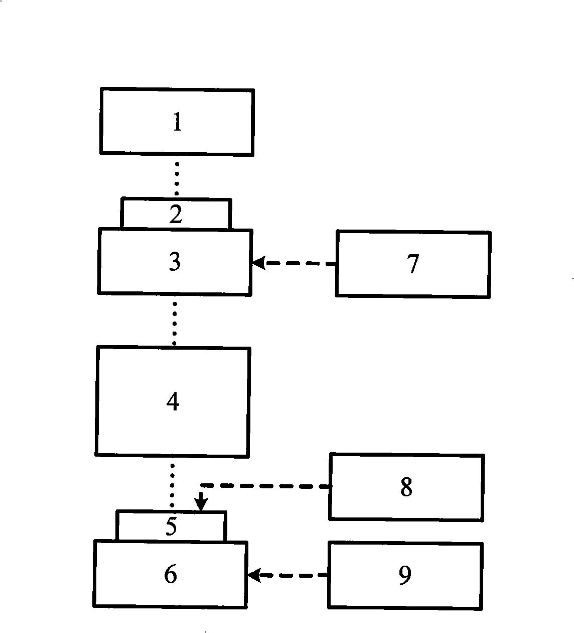
[0019] figure 1 It is a schematic diagram of a lithography apparatus according to a preferred embodiment of the present invention. The apparatus includes: an illumination light source 1 generates and transmits electromagnetic energy, and irradiates the reticle 2 held by the mask stage 3 . Through the objective lens 4, the circuit pattern on the reticle 2 is imaged in the photoresist on the upper surface of the wafer 5, and the workpiece table 6 clamps and drives the wafer 5 to complete horizontal and vertical movement. After the exposed wafer 5 is chemically treated, the pattern on the reticle 2 is transferred to the photoresist on the surface of the wafer 5 . The mask stage motion controller 7 manipulates the three-dimensional movement of the mask stage 3, the workpiece stage vertical controller 8 is used to control the vertical position of ...
PUM
 Abstract
Description
Claims
Application Information
 - R&D Engineer
- R&D Manager
- IP Professional
- Industry Leading Data Capabilities
- Powerful AI technology
- Patent DNA Extraction
Browse by: Latest US Patents, China's latest patents, Technical Efficacy Thesaurus, Application Domain, Technology Topic.
© 2024 PatSnap. All rights reserved.Legal|Privacy policy|Modern Slavery Act Transparency Statement|Sitemap