Light emission device
A light-emitting device and light-emitting layer technology, applied in the direction of electrical components, electric solid-state devices, circuits, etc., can solve the problems that the light-emitting device cannot make sufficient contribution to light emission, attenuation, etc., and achieve the effect of improving light extraction efficiency
- Summary
- Abstract
- Description
- Claims
- Application Information
AI Technical Summary
Problems solved by technology
Method used
Image

Examples
Embodiment approach 1
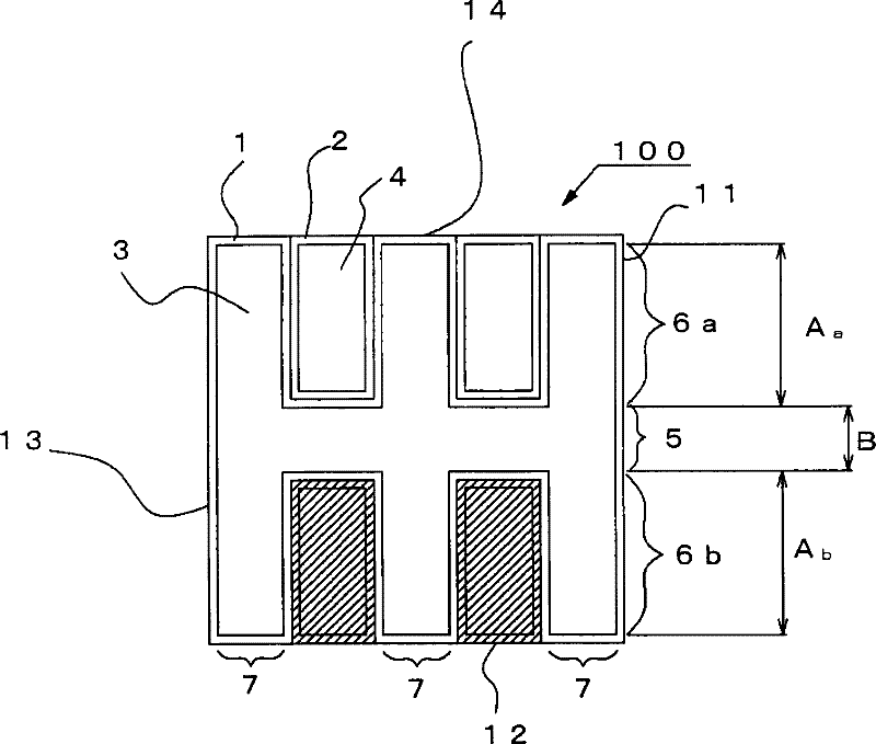
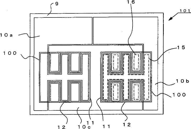
[0059] figure 1 , Figure 2A with Figure 2B It is a schematic plan view showing the semiconductor light emitting element 100 and the light emitting device 101 according to this embodiment.
[0060] figure 1 In the shown semiconductor light emitting element 100, a first semiconductor layer of the first conductivity type and a second semiconductor layer of the second conductivity type are sequentially formed on a light-transmitting substrate, and a part of the first semiconductor layer is exposed from the second semiconductor layer. There are below: a light-emitting region 1 including a stacked structure of the second semiconductor layer and the first semiconductor layer, and an exposed portion 2 , which is an exposed region where the first semiconductor layer is exposed. The second electrode 3 is provided on the surface of the second semiconductor layer in the light-emitting region 1, and the first electrode 4 is provided on the surface of the first semiconductor layer in...
Embodiment approach 2
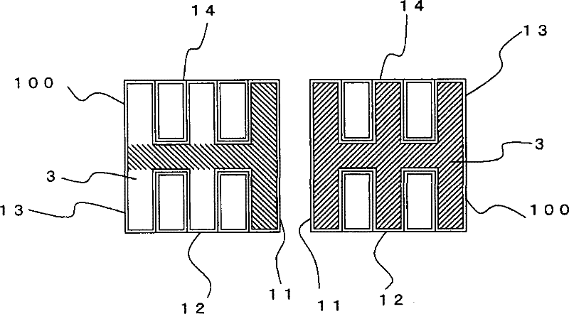
[0098] used in the light-emitting device of Embodiment 2 Figure 5A The light-emitting element shown has a structure including a light-emitting region inside the element and a light-emitting region outside the element. Compared with Embodiment 1, most of the light-emitting regions outside the element are respectively provided on the first side and its opposite side, the adjacent side of the first side, and the extension of the first side and its opposite side are arranged on At both ends of the first side, a part of the side constitutes an extension portion, and the clamping region is formed by extending it. and, Figure 5A The light-emitting element shown has a line-symmetric structure, and its center line is parallel to the first side or its adjacent side on which the second electrode occupying more than half of the side length is disposed. In addition, the second electrode is provided with an external connection area on the adjacent side, extends to the inside of these el...
Embodiment approach 3
[0101] used in the light-emitting device of Embodiment 3 Figure 6AIn the light-emitting element shown, compared with Embodiment 2, the inner second electrode has a wider width and larger area. On the other hand, the width of the clamping region that is a part of the outer second electrode, and the area of each of the above-mentioned regions decrease. Thus, the external connection area of the first electrode is set on the extension of the first side and the two ends of the opposite side connected to each part of the adjacent side, and the clamping area inside the first side and the opposite side. And the extended part becomes a wiring area. As a result, the brightness of light emitted from the end face can be increased in the outer light emitting region, and the front brightness can be increased in the inner light emitting region.
[0102] Figure 6A The light emitting device shown with the Figure 5A Compared with the illustrated light emitting device, the shapes of t...
PUM
 Abstract
Description
Claims
Application Information
 - R&D
- Intellectual Property
- Life Sciences
- Materials
- Tech Scout
- Unparalleled Data Quality
- Higher Quality Content
- 60% Fewer Hallucinations
Browse by: Latest US Patents, China's latest patents, Technical Efficacy Thesaurus, Application Domain, Technology Topic, Popular Technical Reports.
© 2025 PatSnap. All rights reserved.Legal|Privacy policy|Modern Slavery Act Transparency Statement|Sitemap|About US| Contact US: help@patsnap.com