High-voltage semiconductor device and method of fabricating semiconductor high-voltage device
A semiconductor, high-voltage technology, applied in the field of vertical structure semiconductor devices, can solve problems such as degrading device characteristics and changing current paths.
Inactive Publication Date: 2010-11-10
DONGBU HITEK CO LTD
View PDF1 Cites 0 Cited by
- Summary
- Abstract
- Description
- Claims
- Application Information
AI Technical Summary
Problems solved by technology
Therefore, the characteristics of the device are degraded, which may cause a problem that the current path changes after the formation of the later source / drain regions
Method used
View moreImage
Smart ImageViewing Examples

Examples
Embodiment Construction
Login to View More PUM
 Abstract
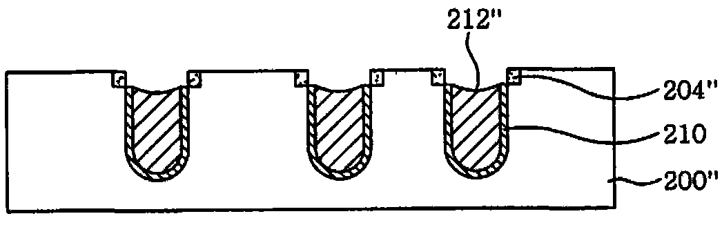
A semiconductor high voltage device comprises; a semiconductor substrate, possessing deep slot; a grid oxide film, forming at side wall of deep slot; a polysilicon layer, forming deep slot and grid oxide film; a partition part, forming on side wall of part of deep slot on grid oxide film. The inventive semiconductor high voltage device can prevent spoilage of grid oxide film during processing andchange of current path such as current leakage between polysilicon upper surface and source / drain.
Description
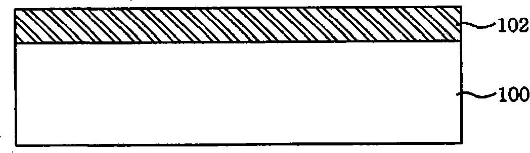
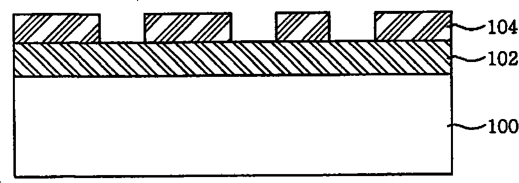
High-voltage semiconductor device and manufacturing method thereof This application claims priority from Korean Patent Application No. 10-2007-0067070 (filed on July 4, 2007) based on 35 U.S.C. §119 and 35 U.S.C. §365, the entire contents of which are hereby incorporated by reference. technical field The present invention relates to a technique of manufacturing a semiconductor device, and more particularly, to a method of manufacturing a semiconductor device of a vertical structure using a high voltage. Background technique Since high voltage semiconductor devices require high voltages compared to complementary metal oxide semiconductor (CMOS) devices, high voltage semiconductor devices may generally have a vertical structure. For example, in the process of manufacturing CMOS, a voltage of about 1.5V may be used. On the other hand, in the process of manufacturing high voltage devices, a voltage of 10V to 100V, preferably 30V, may be used. In order to achieve the purpose...
Claims
Login to View More Application Information
Patent Timeline
 Patent Type & Authority Patents(China)
IPC IPC(8): H01L21/336H01L21/311H01L21/28
CPCH01L21/3083H01L29/66621H01L21/0274
Inventor 河丞撤
Owner DONGBU HITEK CO LTD
Features
- R&D
- Intellectual Property
- Life Sciences
- Materials
- Tech Scout
- Unparalleled Data Quality
- Higher Quality Content
- 60% Fewer Hallucinations
Learn More Browse by: Latest US Patents, China's latest patents, Technical Efficacy Thesaurus, Application Domain, Technology Topic, Popular Technical Reports.
© 2025 PatSnap. All rights reserved.Legal|Privacy policy|Modern Slavery Act Transparency Statement|Sitemap|About US| Contact US: help@patsnap.com