Delay locked loop circuit and method for eliminating jitter and offset therein
A delay-locked loop, signal-to-signal technology, applied in the direction of electrical components, automatic power control, etc., to achieve high resolution, stable operation, and reduce production costs and size.
- Summary
- Abstract
- Description
- Claims
- Application Information
AI Technical Summary
Problems solved by technology
Method used
Image


Examples
Embodiment Construction
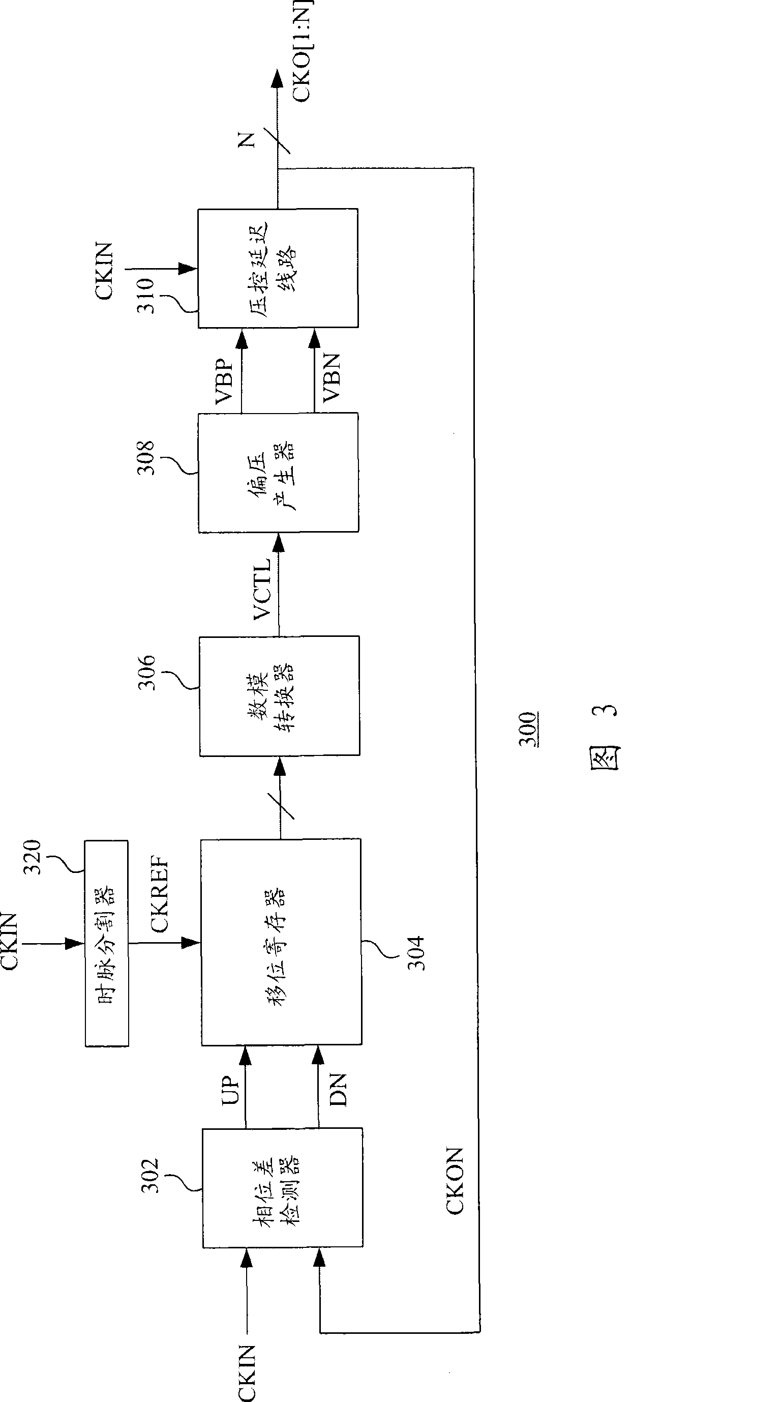
[0036] FIG. 3 is a schematic diagram showing a delay locked loop circuit according to an embodiment of the present invention. The delay locked loop (delay locked loop, DLL) circuit 300 includes: a phase difference detector (phasedifference detector) 302, a clock divider (divider) 320, a shift register 304, a digital-to-analog converter (DAC) 306, a bias generator device 308 and the voltage control unit. In this embodiment, the voltage control unit is a voltage controlled delay line (voltage controlled delay line, VCDL) 310 . The phase difference detector 302 is used to detect the phase difference between the input clock signal CKIN and the feedback clock signal CKON, and has two output terminals UP and DN. The output of the phase difference detector 302 is a pulse signal, and the pulse width of the pulse signal is the same as that of the signal CKIN leading or delaying the signal CKON. When the signal CKIN leads the signal CKON, the pulse signal will be output from the outpu...
PUM
 Abstract
Description
Claims
Application Information
 - R&D
- Intellectual Property
- Life Sciences
- Materials
- Tech Scout
- Unparalleled Data Quality
- Higher Quality Content
- 60% Fewer Hallucinations
Browse by: Latest US Patents, China's latest patents, Technical Efficacy Thesaurus, Application Domain, Technology Topic, Popular Technical Reports.
© 2025 PatSnap. All rights reserved.Legal|Privacy policy|Modern Slavery Act Transparency Statement|Sitemap|About US| Contact US: help@patsnap.com