Method for measuring nanometer electronic thin film micro-zone piezoelectric coefficient based on atomic microscope

An atomic force microscope and piezoelectric coefficient technology, which is applied in the field of materials, can solve the problems of uneven piezoelectric effect, difficult to accurately detect the number of charges, and limited piezoelectric coefficient in nano-micro area, and achieve the effect of simple operation.

Inactive Publication Date: 2009-07-29
UNIV OF ELECTRONICS SCI & TECH OF CHINA
View PDF0 Cites 24 Cited by
  • Summary
  • Abstract
  • Description
  • Claims
  • Application Information

AI Technical Summary

Problems solved by technology

[0005] Although the above-mentioned macroscopic measurement methods of piezoelectric coefficients are very mature, these methods are limited in the measurement of piezoelectric coefficients in nanometer micro-regions.
For example, the optical detection method (Michael interferometry and ATR method) is impossible to identify the deformation in the submicron region due to the limitation of the wavelength; the scanning near-field microwave microscopy method can only reach a minimum resolution of 100nm due to the limitation of the size of the microwave resonator. Moreover, due to the existence of grain boundaries for independent nano-piezoelectric structures (nano-islands or nano-grains) on the order of 100nm, the piezoelectric effect presents inhomogeneity in the nanoscale. The electric coefficient is just the average result of the non-uniform distribution of piezoelectric properties in the resonator
Methods that rely on charge detection such as quasi-static methods are also very limited in detecting deformation in submicron regions. For example, in a 50nm square region, the number of charges generated by the positive piezoelectric effect is less than 10 -14 ~10 -17 C level, coupled with the influence of external current noise, the amount of charge is basically difficult to be accurately detected
So far, there is no method to measure the piezoelectric coefficient of nanopiezoelectric materials in a micro-region smaller than 100nm

Method used


Image

  • Method for measuring nanometer electronic thin film micro-zone piezoelectric coefficient based on atomic microscope
  • Method for measuring nanometer electronic thin film micro-zone piezoelectric coefficient based on atomic microscope
  • Method for measuring nanometer electronic thin film micro-zone piezoelectric coefficient based on atomic microscope

Examples


Embodiment Construction

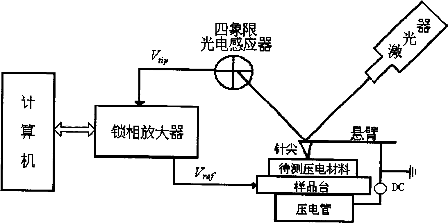
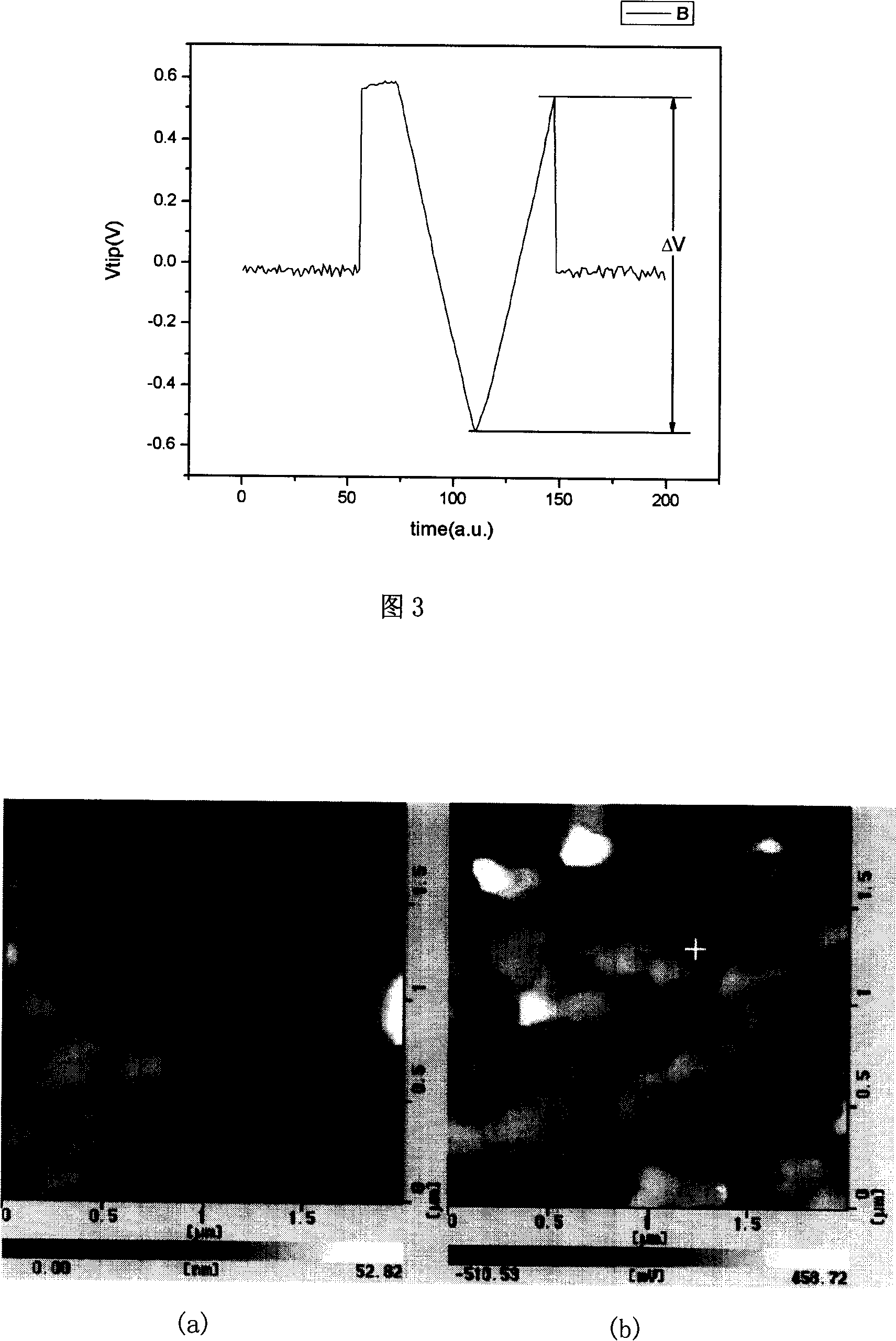
[0027] according to figure 1 The measurement system is built as shown, the computer is connected to the lock-in amplifier SR830 through the GPIB bus, and the internal reference oscillation signal V of the lock-in amplifier is ref It is connected with the conductive sample stage of the atomic force microscope, and the conductive tip of the atomic force microscope is grounded ( figure 1 ). First, calibrate the sensitivity S of the photoelectric sensor. When correcting, first contact the needle tip with the rigid sample, control the piezoelectric tube to move up and down a certain distance H, and measure the voltage change range ΔV through the four-quadrant photoelectric sensor, and then get the sensitivity S=H / ΔV (as shown in Figure 3); then place the piezoelectric material to be measured on the sample stage, and apply the AC voltage V generated by the internal oscillator of the lock-in amplifier between the "conductive needle tip-the piezoelectric material to be measured-samp...


PUM


Abstract

The invention discloses a method for measuring the piezoelectric coefficient of a nano-electronic thin film micro area based on an atomic force microscope, which relates to the analysis and characterization of the physical and chemical properties of materials, in particular to a method for measuring the piezoelectric coefficient of a thin film material based on the atomic force microscope. AC voltage Vref is imposed on a piezoelectric material to be measured for generating a deformation Sigma=d question mark Vref; by using the optical lever system of the atomic force microscope, the deformation Sigma is converted into an electrical signal Vtip= S question mark Sigma; and then Vd=G question mark Vtip is obtained by amplification of a lock-phase amplifier; finally, the micro-area piezoelectric coefficient (see the formula) of the piezoelectric material to be measured is obtained by calculation. The invention realizes the micro-area piezoelectric coefficient measurement of a thin-film sample within a nano-scale scope, and thus enlarges the application scope of the atomic force microscope; the entire measurement method is simple and easy for mastering.

Description

technical field [0001] The invention belongs to the technical field of materials, and relates to the analysis and characterization of physical and chemical properties of materials, in particular to a method for measuring the piezoelectric coefficient of thin film materials based on an atomic force microscope. Background technique [0002] Piezoelectric effect refers to the phenomenon that materials generate electric charges under the action of external pressure (called positive piezoelectric effect) or produce mechanical deformation under the action of external voltage (called inverse piezoelectric effect). Manifestations. Materials with pronounced piezoelectric effect are called piezoelectric materials. The charge generated by piezoelectric materials under the action of unit pressure or the amount of deformation generated under unit voltage is called the piezoelectric coefficient, which is used to measure the magnitude of the piezoelectric effect. The piezoelectric coeffi...

Claims


Application Information

Patent Timeline
Patent Type & Authority Applications(China)
IPC IPC(8): G01R29/22
Inventor 李言荣王志红曾慧中孙浩明古曦
Owner UNIV OF ELECTRONICS SCI & TECH OF CHINA
Why Eureka
Try Eureka