X-ray imaging device
An imaging device and X-ray technology, applied in the field of X-ray imaging, can solve the problems of speed affecting diagnosis, particle size limitation, time-consuming film development, etc., to achieve the effect of improving imaging quality
- Summary
- Abstract
- Description
- Claims
- Application Information
AI Technical Summary
Problems solved by technology
Method used
Image

Examples
Embodiment Construction
[0011] The present invention will be further described in detail below in conjunction with the accompanying drawings.
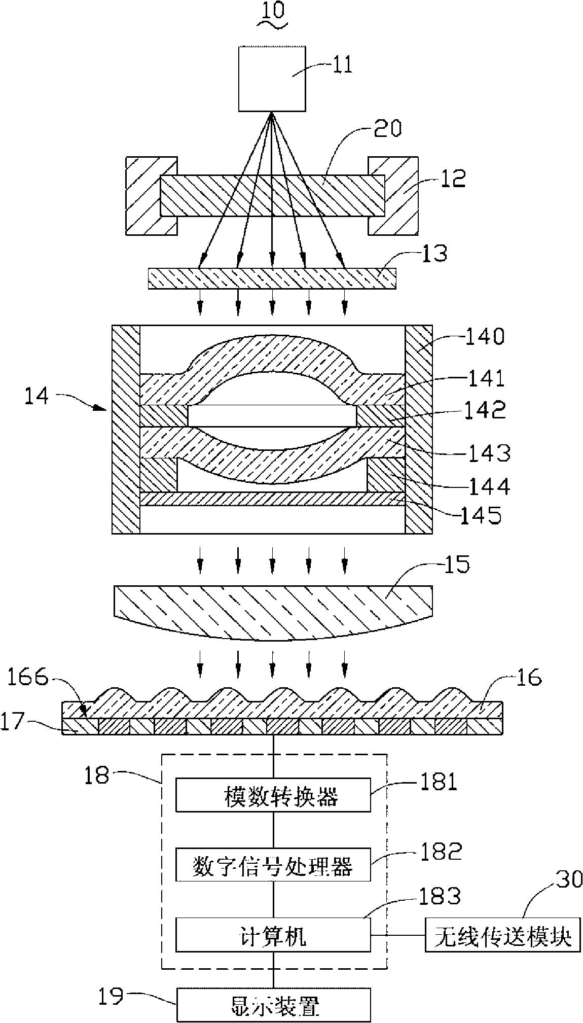
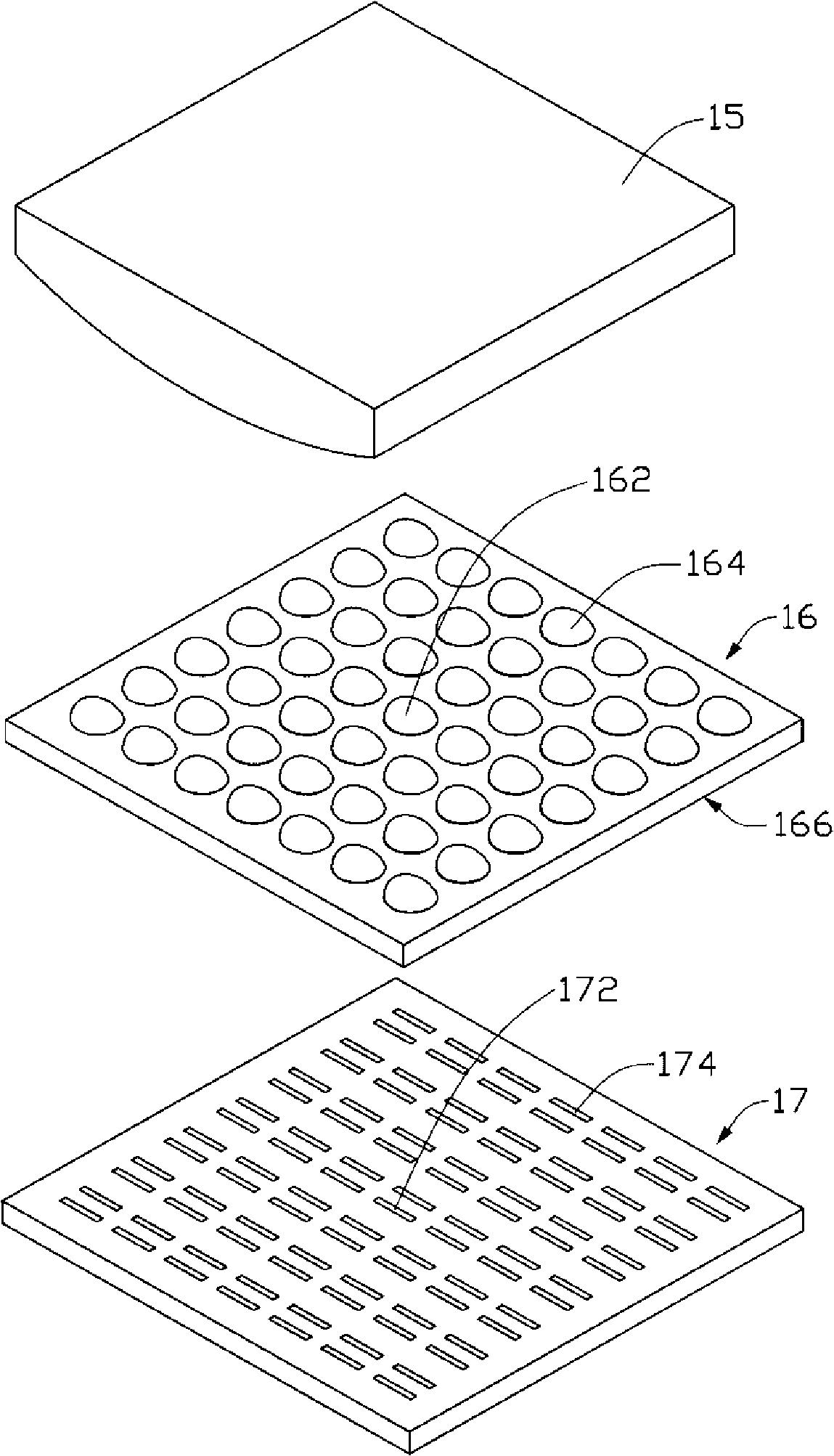
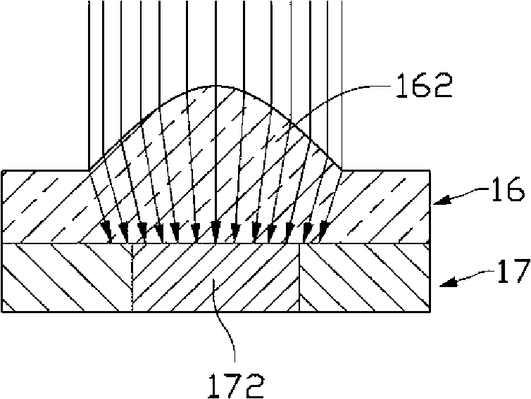
[0012] see figure 1 , shown as the X-ray imaging device 10 of the embodiment of the present invention comprises an X-ray light source 11, a carrying table 12, a fluorescent screen 13, a lens module 14, a correction lens 15, an optical leveling element (OpticalLeveling Layer) ) 16, an image sensor 17, an image signal processing module 18, and a display device 19. The image sensor 17 is electrically connected to the image signal processing module 18 , and the image signal processing module 18 is electrically connected to the display device 19 .
[0013] The X-ray light source 11 can use a copper target. The working voltage of the X-ray light source 11 is between 10 kV and 100 kV, preferably, the working voltage is between 20 kV and 60 kV. The operating current of the X-ray light source 11 is between 0.01 mA and 1 mA, preferably, the operating current is betw...
PUM
 Abstract
Description
Claims
Application Information
 - R&D
- Intellectual Property
- Life Sciences
- Materials
- Tech Scout
- Unparalleled Data Quality
- Higher Quality Content
- 60% Fewer Hallucinations
Browse by: Latest US Patents, China's latest patents, Technical Efficacy Thesaurus, Application Domain, Technology Topic, Popular Technical Reports.
© 2025 PatSnap. All rights reserved.Legal|Privacy policy|Modern Slavery Act Transparency Statement|Sitemap|About US| Contact US: help@patsnap.com