Supercharge Your Innovation With Domain-Expert AI Agents!

Method and system of handling silicon-based wafer and method of packaging semiconductor

A silicon-based crystal, silicon-based technology, applied in the direction of semiconductor devices, semiconductor/solid-state device manufacturing, semiconductor/solid-state device components, etc., can solve the difficulty, inconvenience and loss of through-silicon vias in the flip-chip bonding process. And other issues

Active Publication Date: 2009-10-28
TAIWAN SEMICON MFG CO LTD
View PDF0 Cites 6 Cited by
  • Summary
  • Abstract
  • Description
  • Claims
  • Application Information

AI Technical Summary

Problems solved by technology

However, after the glass carrier 20 is removed, the subsequent flip-chip bonding process becomes difficult because the TSV interposer is easily broken, and many TSV interposers are damaged. loss
[0006] It can be seen that the above-mentioned existing method and system for processing silicon-based wafers and the method for packaging semiconductor elements obviously still have inconvenience and defects in structure and use, and need to be further improved urgently.
In order to solve the above-mentioned problems, the relevant manufacturers have tried their best to find a solution, but no suitable design has been developed for a long time, and the general products do not have a suitable structure to solve the above-mentioned problems. This is obviously related. The problem that the industry is eager to solve

Method used


Image

  • Method and system of handling silicon-based wafer and method of packaging semiconductor
  • Method and system of handling silicon-based wafer and method of packaging semiconductor
  • Method and system of handling silicon-based wafer and method of packaging semiconductor

Examples


Embodiment Construction

[0063] In order to further explain the technical means and effects of the present invention to achieve the intended purpose of the invention, the method and system for processing silicon-based wafers and the method for packaging semiconductor elements proposed according to the present invention will be described below in conjunction with the accompanying drawings and preferred embodiments. Its specific implementation, structure, feature and effect thereof are described in detail as follows.

[0064] The aforementioned and other technical contents, features and effects of the present invention will be clearly presented in the following detailed description of preferred embodiments with reference to the drawings. For convenience of description, in the following embodiments, the same elements are denoted by the same numbers.

[0065] Some embodiments of the present invention will be described in detail as follows. However, in addition to the following descriptions, the present i...


PUM


Abstract

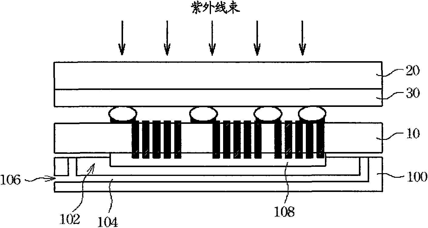
The invention relates to a method and a system of handling a silicon-based wafer and a method of packaging semiconductor. A silicon-based wafer has a first and second surfaces wherein a glass carrier is mounted on the second surface by a UV tape. The method of handling a silicon-based wafer comprises holding the silicon-based wafer by a vacuum holder applied on the first surface of the silicon-based wafer; removing said glass carrier from the silicon-based wafer by irradiating said UV tape with a UV beam through the glass carrier, thereby releasing the UV tape; flipping the silicon-based wafer; placing the silicon-based wafer onto a vacuum plate; securing the silicon-based wafer on the vacuum plate by applying vacuum to the vacuum plate; and releasing the vacuum holder from the silicon-based wafer. The invention further provides a method of packaging a semiconductor and a system of handling a silicon-based wafer. A rigidity demanded by the silicon-based wafer from which the glass carrier is removed is provided by vacuum substrate, thereby reducing breakage of the medium layer in the through-silicon medium window.

Description

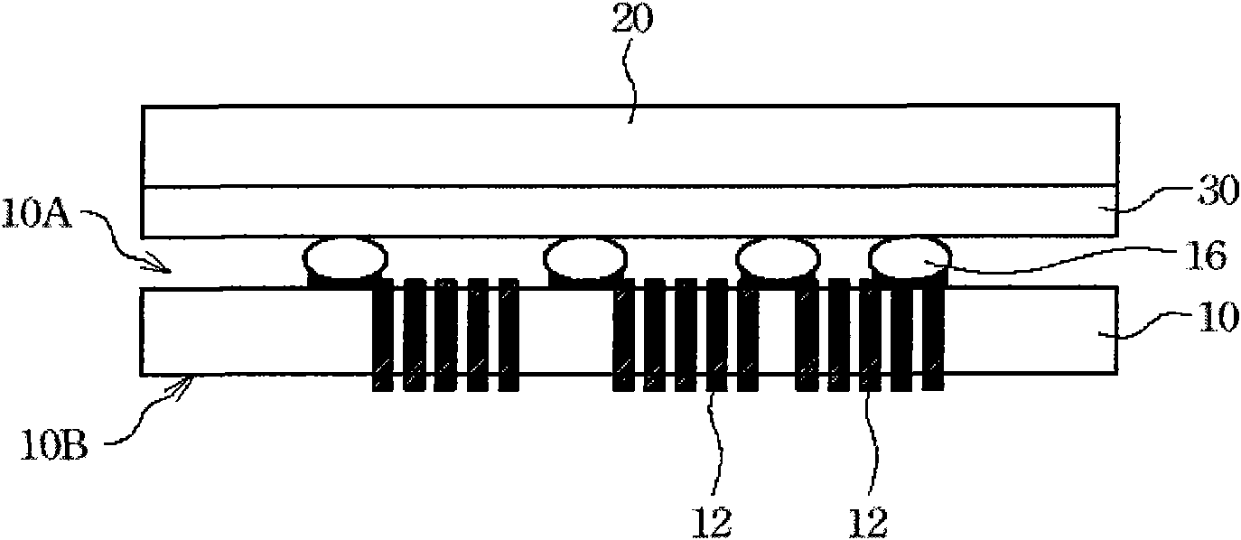
technical field [0001] The invention relates to a packaging and assembly technology for semiconductor elements, in particular to a method and system for processing silicon-based wafers and a method for packaging semiconductor elements. Background technique [0002] One of the recent developments in microelectronics packaging technology is Through-Silicon-Via Interposers (TSV Interposers), which allow denser component chips because they allow three-dimensional stacking. encapsulation. However, due to the very thin thickness of the TSV interposer, the handling of the TSV interposer is challenging during the wafer assembly process. Typically, the TSV interposer is fabricated from a silicon wafer and has a thickness of 90 microns. [0003] see Figure 10 Shown is a schematic cross-sectional view of a glass carrier adhered to the TSV interposer with UV-irradiated adhesive tape and removed from the TSV interposer by ultraviolet light. The silicon-based wafer 10 of the TSV inter...

Claims


Application Information

Patent Timeline
Patent Type & Authority Applications(China)
IPC IPC(8): H01L21/50H01L21/58H01L21/00H01L21/683
CPCH01L2224/13316H01L2924/01023H01L2924/01082H01L2224/81193H01L2221/68381H01L2224/97H01L2224/81005H01L24/97H01L25/0655H01L21/67184H01L2924/15311H01L2924/01029H01L21/6835H01L2221/68331H01L21/486H01L21/67207H01L2224/75744H01L24/81H01L2224/81815H01L23/49827H01L23/147H01L2924/01005H01L2924/01033H01L2924/01075H01L24/75H01L2224/16235H01L2924/0105
Inventor 李建勋陈承先李明机郭祖宽
Owner TAIWAN SEMICON MFG CO LTD
Features
  • R&D
  • Intellectual Property
  • Life Sciences
  • Materials
  • Tech Scout
  • Unparalleled Data Quality
  • Higher Quality Content
  • 60% Fewer Hallucinations
Learn More