Monitor burn-in test device and monitor burn-in test method

A technology of aging test and temperature test, which is applied in the direction of measuring device, digital circuit test, electronic circuit test, etc. It can solve the problems that the heater cannot fully contact the test object and the heater lacks versatility.

Inactive Publication Date: 2009-12-09
FUJITSU LTD
View PDF7 Cites 2 Cited by
  • Summary
  • Abstract
  • Description
  • Claims
  • Application Information

AI Technical Summary

Problems solved by technology

Therefore, for example, when the size of the test object blocking the bottom surface of the metal pipe increases, the bottom surface of the heater cannot contact the test object with a sufficient area.
Such heaters lack versatility

Method used


Image

  • Monitor burn-in test device and monitor burn-in test method
  • Monitor burn-in test device and monitor burn-in test method
  • Monitor burn-in test device and monitor burn-in test method

Examples


Embodiment Construction

[0054] Hereinafter, an embodiment of the present invention will be described with reference to the drawings.

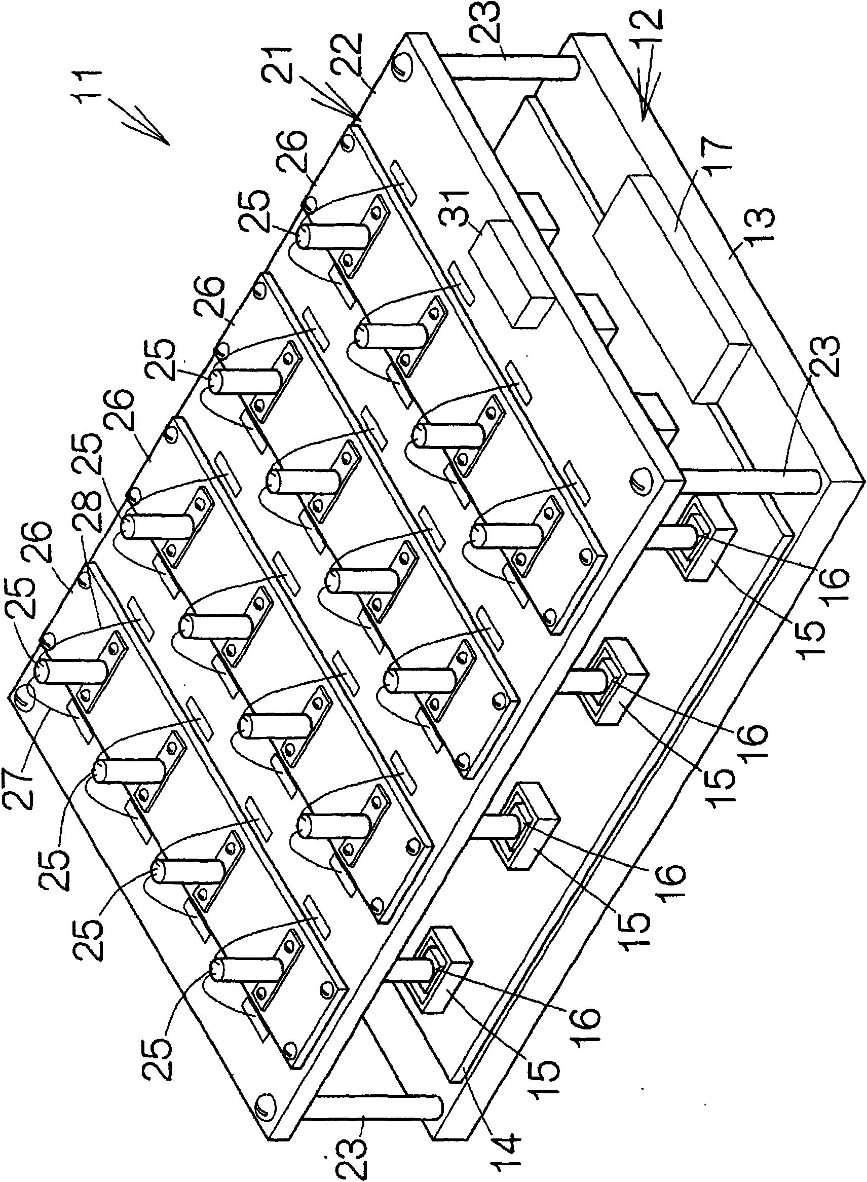
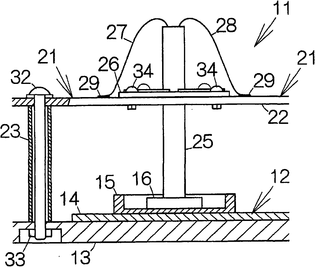
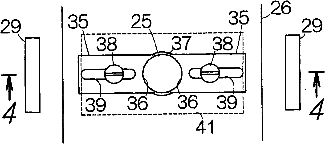
[0055] figure 1 A monitoring aging test device 11 according to an embodiment of the present invention is schematically shown. This monitoring aging test device 11 has an aging board 12 . The burn-in board 12 has, for example, a resin-made board main body 13 . A printed circuit board 14 is fixed to the board main body 13 . The printed circuit board 14 defines an outline inside the outline of the board main body 13 . A plurality of sockets 15 are mounted on the surface of the printed circuit board 14 . The sockets 15 are arranged, for example, in 4 rows and 4 columns.

[0056] A component 16 to be tested is attached to each socket 15 . The elements 16 are all composed of the same semiconductor device. The element 16 includes memory chips such as SDRAM chips that require refresh processing. On the outside of the printed circuit board 14 , a connector 17 is attach...


PUM


Abstract

The invention provides a monitor burn-in test device and a monitor burn-in test method. In a monitor burn-in test device (11), data is written all at once into a plurality of elements (16) requiring a refresh process. The refresh process is performed in the elements (16) after the write process. The data is held. When performing a read-out process, the refresh process is interrupted in the element (16) from which read-out is to be performed. Data is read out from the interrupted element (16). Thus, the refresh process is interrupted only in the element (16) from which read-out is to be performed. Accordingly, the refresh process can be continued in the element (16) other than the element from which read-out is to be performed. Thus, the data is surely held. The data write-in process may be completed at once. Thus, the monitor burn-in test can be effectively performed.

Description

technical field [0001] The present invention relates to a monitoring aging test device used, for example, in a monitoring aging test. Background technique [0002] For example, a so-called monitor burn-in test is performed before product shipment of semiconductor devices such as SRAMs. In practice, a plurality of semiconductor devices of the test object are mounted on a burn-in board. The semiconductor device is heated by, for example, a heater. Semiconductor devices are maintained at a high temperature of, for example, 100 degrees Celsius. At this time, the semiconductor device is driven. A voltage of a higher value than usual is applied to the semiconductor device. The operation of the semiconductor device is checked in this way. [0003] When carrying out the operation check in the monitor burn-in test, first, (1) carry out the writing and reading process. In this step, data write processing and read processing are performed. At this time, the written data is compa...

Claims


Application Information

Patent Timeline
IPC IPC(8): G11C29/56G11C11/406G11C11/401G11C29/08G01R31/26
CPCG11C29/56G11C29/08G11C29/06G01R31/319G11C29/56016G01R31/287G01R31/2875G11C11/406G11C11/401
Inventor 前崎义博勅使河原宽小平幸彦关口尚枝
Owner FUJITSU LTD
Why Eureka
Try Eureka