Wet etching stripping method of SiC-substrate GaN-based LED

A wet etching and substrate technology, which is applied in the field of optoelectronics, can solve the problems of low reliability and low power, and achieve the effect of improving light extraction efficiency, significant effect and brightness improvement

Active Publication Date: 2010-08-04
枣庄科顺数码有限公司
View PDF6 Cites 13 Cited by
  • Summary
  • Abstract
  • Description
  • Claims
  • Application Information

AI Technical Summary

Problems solved by technology

[0011] The present invention aims at the existing problems of low reliability and low power in the production of LEDs based on SiC or Si as substrat

Method used


Image

  • Wet etching stripping method of SiC-substrate GaN-based LED
  • Wet etching stripping method of SiC-substrate GaN-based LED
  • Wet etching stripping method of SiC-substrate GaN-based LED

Examples


Embodiment Construction

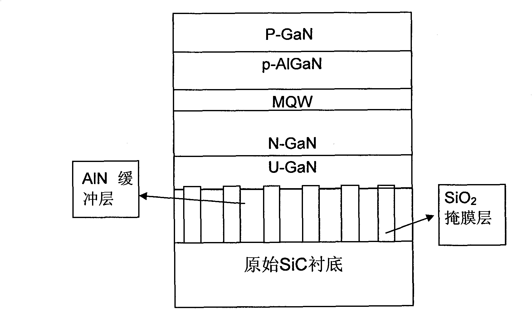
[0024]The wet etching and stripping manufacturing method of SiC substrate GaN-based LED of the present invention comprises the following three parts of the manufacturing process:

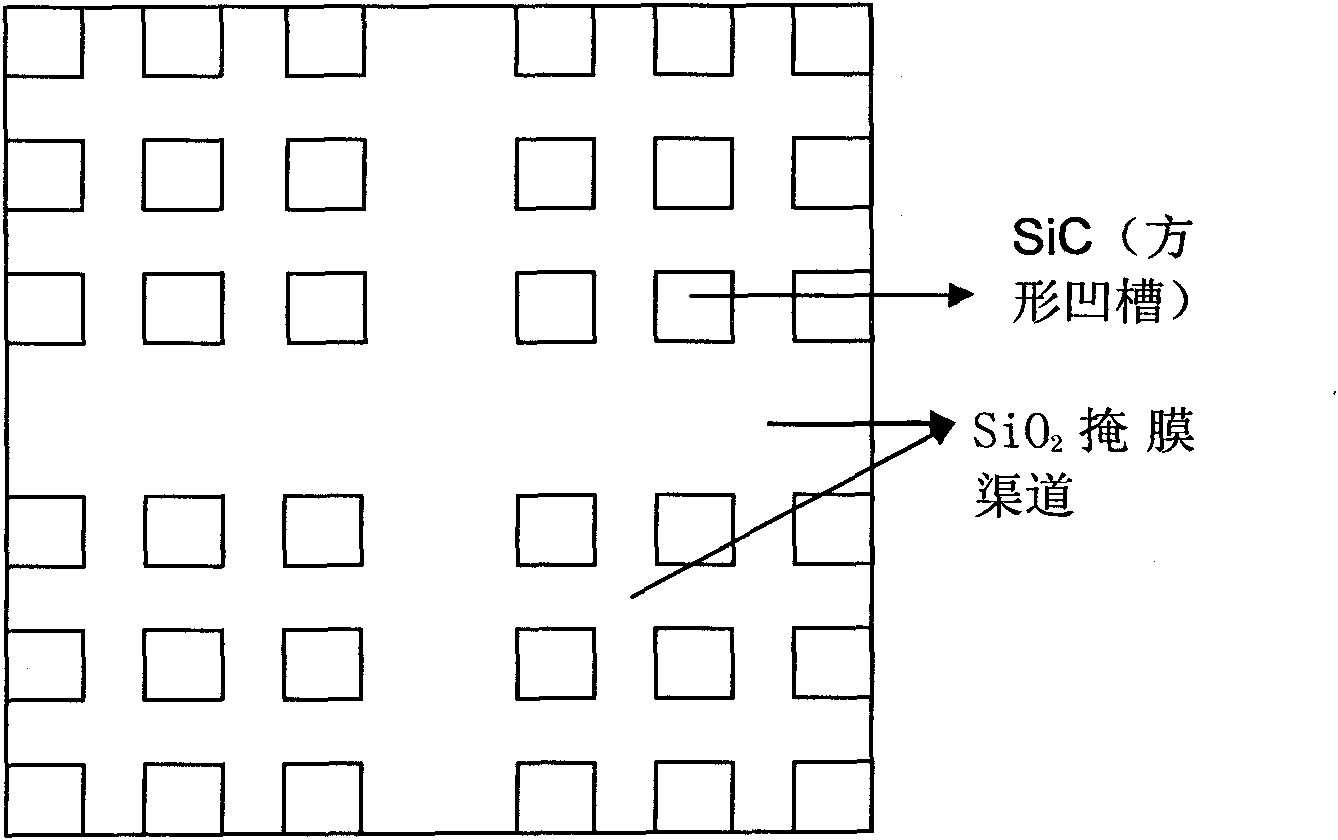
[0025] 1. Make the original SiC substrate pattern

[0026] (1) Put the original SiC substrate (different from ordinary sapphire substrate) into PECVD (plasma enhanced chemical vapor deposition) equipment, and evaporate a layer thickness of 1000 -3000 SiO 2 mask;

[0027] (2) Take out the evaporated SiO 2 After masking the original SiC substrate, the SiO 2 Coat photoresist on the mask, use the pre-engraved pattern mask on the SiO 2 On the mask, use a photolithography machine to carve the designed SiO that can form criss-cross patterns. 2 Graphics of the mask channel;

[0028] (3) developing;

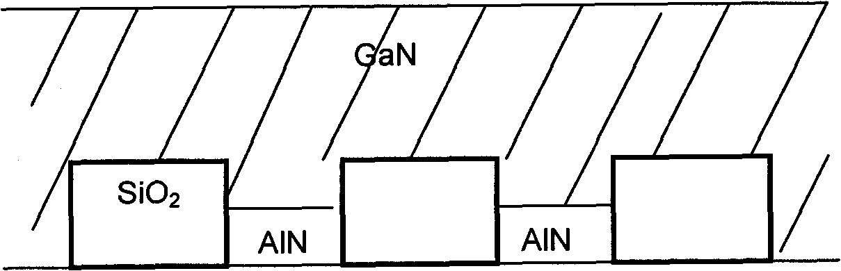
[0029] (4) After development, use HF acid to etch away the SiO without photoresist 2 Mask, so that these parts expose the original SiC substrate surface, get figure 1 The square grooves shown are on...


PUM


Abstract

The invention discloses a wet etching stripping method of a SiC-substrate GaN-based LED, which comprises the following steps: (1) manufacturing an original SiC substrate pattern, evaporating a SiO2 mask on an original SiC substrate, spreading a photoresist on the SiO2 mask, etching the designed pattern on the SiO2 by using a photoetching machine, and after developing, forming interlaced SiO2 mask channels by etching with HF acid and acetone; (2), growing an epitaxial wafer with a conventional structure by using a conventional method on the original SiC substrate on which the pattern is etched; and (3) manufacturing an inverted epitaxial wafer, plating a layer of reflective metal on the surface of the epitaxial wafer, bonding the reflective metal layer on a new SiC or Si substrate, and stripping the original SiC substrate by etching to obtain the SiC-substrate LED stripped by inverted etching. The method can successfully strip the original SiC substrate, coarsen the surface of the GaN-based LED, improve the power of the GaN-based LED by 80 to 120 percent, and manufacture large-power elements and LED lamps.

Description

technical field [0001] The invention relates to a stripping method for wet etching and stripping of a GaN-based LED on a SiC substrate, and belongs to the field of optoelectronic technology. Background technique [0002] In 1998, Lumileds packaged the world's first high-power LED (1W LUXOEN device), which made LED devices change from the previous application of indicator lights to a new type of solid light source that can replace traditional lighting, triggering the development of human history since the invention of incandescent lamps. Another lighting revolution. 1WLUXOEN devices make the power of LED jump from tens of milliwatts to more than 1000 milliwatts, and the luminous flux of a single device also leaps from less than 1 lm to more than ten lm. [0003] Due to the high power density of the high-power LED chip, the designer and manufacturer of the device must optimize the thermal system of the device in terms of structure and materials. At present, there are two typ...

Claims


Application Information

Patent Timeline
IPC IPC(8): H01L33/00
Inventor 吴德华朱学亮李树强王成新徐现刚
Owner 枣庄科顺数码有限公司
Why Eureka
Try Eureka