
Micro mirror layer, liquid crystal on silicon (LCOS) display device and manufacturing method thereof

A technology of micro-mirror and backing layer, applied in semiconductor/solid-state device manufacturing, optics, instruments, etc., can solve the problems of decreased reflectivity of aluminum reflective surface, difficulty of aluminum reflective surface, etc., and achieve the effect of high process technology

Active Publication Date: 2010-10-20
SEMICON MFG INT (SHANGHAI) CORP
View PDF0 Cites 4 Cited by
  • Summary
  • Abstract
  • Description
  • Claims
  • Application Information

AI Technical Summary

Problems solved by technology

[0004] With the continuous improvement of the integration of semiconductor devices, it is more and more difficult to form a high-reflectivity aluminum reflective surface, especially when the process reaches below 0.13 microns, without changing the total area of ​​the micro-mirror layer, increasing the micro-mirror The number of pixels is used to improve the resolution of pixels, thereby reducing the area of ​​a single micro-mirror, which will cause the reflectivity of the aluminum reflective surface to decrease

Method used


Image

  • Micro mirror layer, liquid crystal on silicon (LCOS) display device and manufacturing method thereof
  • Micro mirror layer, liquid crystal on silicon (LCOS) display device and manufacturing method thereof
  • Micro mirror layer, liquid crystal on silicon (LCOS) display device and manufacturing method thereof

Examples


Embodiment Construction

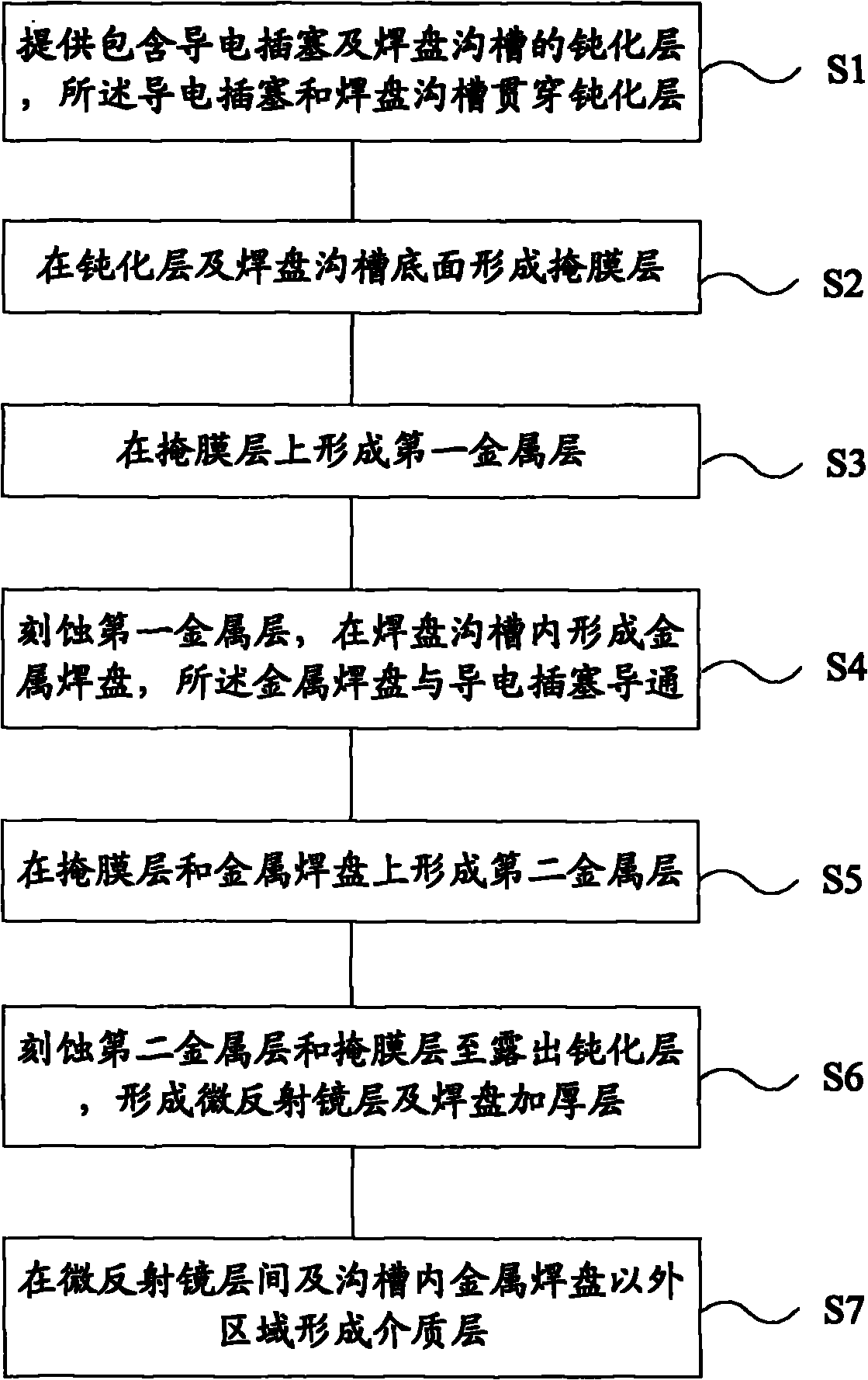
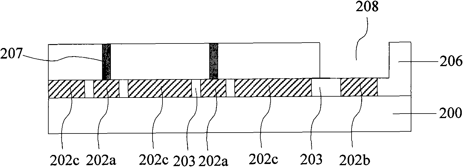
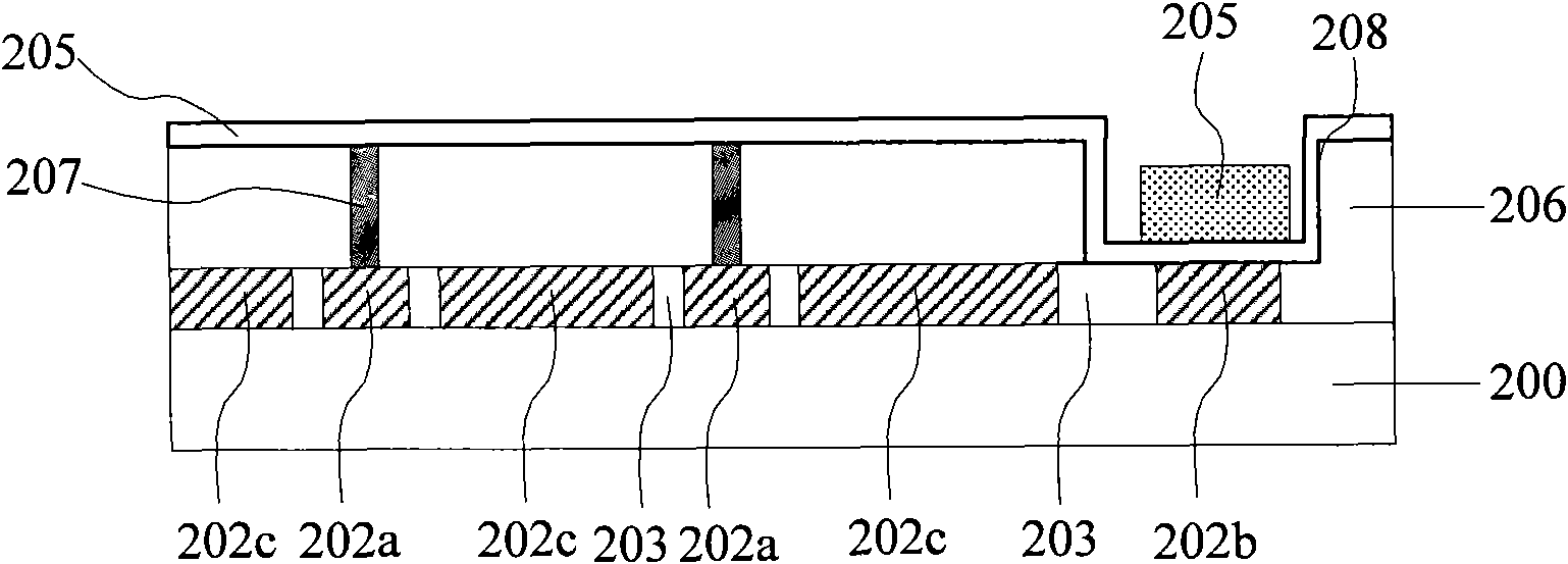
[0014] figure 1 It is a flow chart of a specific embodiment of the present invention for fabricating the micro-mirror surface in a silicon-based liquid crystal display device. Such as figure 1 As shown, step S1 is executed to provide a passivation layer including conductive plugs and pad grooves, and the conductive plugs and pad grooves penetrate the passivation layer; step S2 is executed to provide a passivation layer on the passivation layer and pad grooves. A mask layer is formed on the bottom surface; step S3 is performed to form a first metal layer on the mask layer; step S4 is performed to etch the first metal layer to form a metal pad in the pad groove, and the metal pad is connected to the conductive The plug is turned on; step S5 is performed to form a second metal layer on the mask layer and the metal pad; step S6 is performed to etch the second metal layer and the mask layer to expose the passivation layer to form a micromirror layer and Retaining the second metal...


PUM

PropertyMeasurementUnit
Thicknessaaaaaaaaaa
Thicknessaaaaaaaaaa

Abstract

The invention provides a micro mirror layer, a liquid crystal on silicon (LCOS) display device and a manufacturing method thereof, wherein the method for manufacturing the micro mirror layer comprises the following steps that: a passivating layer comprising a conducting plug and a pad groove is provided, and the conducting plug and the pad groove penetrate through the passivating layer; a masking film layer is formed at the passivating layer and the bottom surface of the pad groove; a first metal layer is formed on the masking film layer; the first metal layer is etched, and a metal pad is formed in the pad groove and is conducted with the conducting plug; a second metal layer is formed on the masking film layer and the metal pad; the metal layer and the masking film layer are etched till the passivating layer is exposed so as to form the micro mirror layer, and the second metal layer on the metal pad is retained; and a dielectric layer is formed in the micro mirror layer and the area beyond the metal pad in the groove. The invention can form an even and thin micro mirror layer.

Description

technical field [0001] The invention relates to a micro-mirror layer, a liquid crystal on silicon (LCOS) display device and a manufacturing method thereof. Background technique [0002] Liquid crystal on silicon (LCOS) is a new type of reflective liquid crystal display device. Unlike ordinary liquid crystals, LCOS combines CMOS technology to directly realize the driving circuit on the silicon wafer, and uses CMOS technology to make the active pixel matrix on the silicon substrate. On the bottom, it has the characteristics of small size and high resolution. [0003] An ideal LCOS should be flat, smooth and have a high reflectivity, so that it can ensure a good liquid crystal alignment and consistency of liquid crystal layer thickness, without distorting light, which requires that the reflective mirror surface must be quite flat. The ability to precisely control the reflected light path is a critical factor for high-end applications such as projection TVs. [0004] With the ...

Claims


Application Information

Patent Timeline
IPC IPC(8): G02F1/1362H01L21/02H01L21/822
Inventor 刘煊杰陈宇涵郭亮良
Owner SEMICON MFG INT (SHANGHAI) CORP
Learn More