Silicon-based photonic crystal channel-shaped waveguide micro-cavity laser
A photonic crystal slot and photonic crystal technology, which is applied to the structure of optical waveguide semiconductor and the structure of optical resonant cavity, can solve the problems of different chemical and physical properties, low luminous efficiency, incompatible manufacturing process, etc., and achieve enhanced luminous efficiency. , high quality factor, low mode volume effect
- Summary
- Abstract
- Description
- Claims
- Application Information
AI Technical Summary
Problems solved by technology
Method used
Image

Examples
Embodiment 1
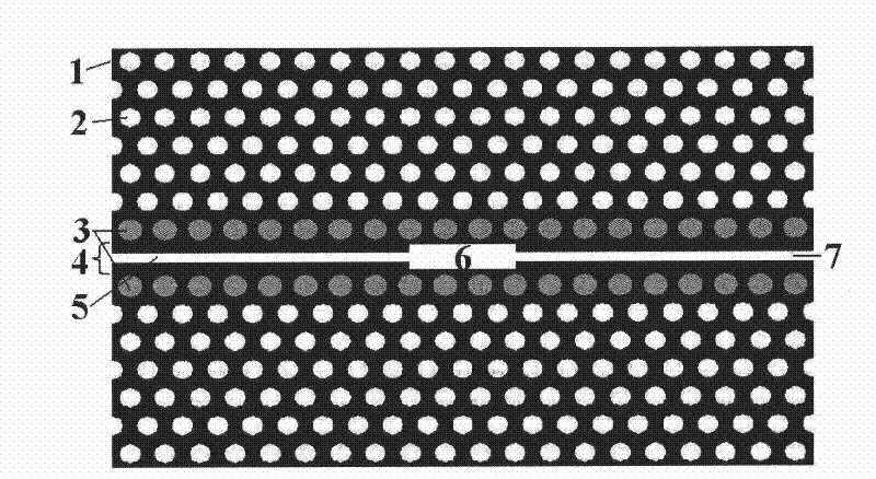
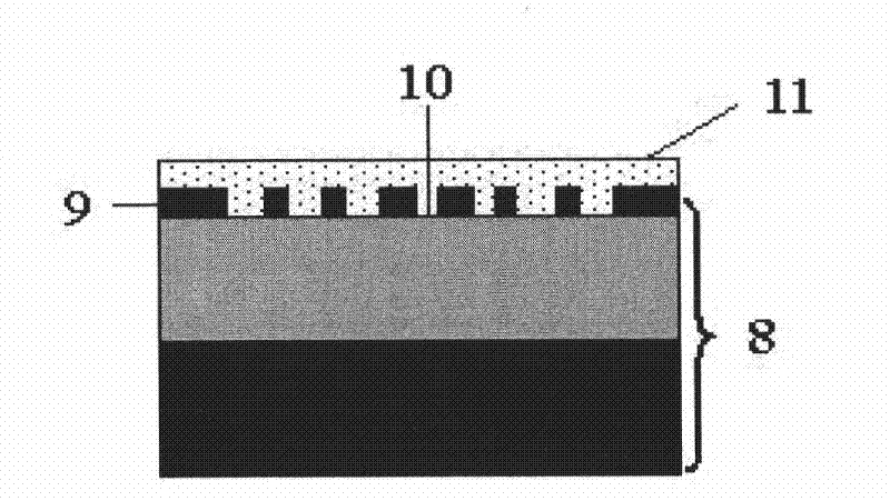
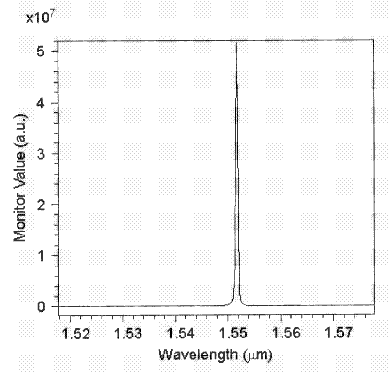
[0041]In this embodiment, the luminescent material whose refractive index is lower than that of the silicon on the top layer of the SOI substrate filled in the groove-shaped waveguide and the air hole is the silicon dioxide material doped with erbium ions, and the silicon dioxide material doped with erbium is produced by the sol-gel method. The luminescence peak of the prepared erbium-doped silicon dioxide material is around 1550 nm. The two-dimensional slab photonic crystal is an asymmetric oxide cladding slab triangular lattice photonic crystal structure, the lattice constant a=409.16nm, the air hole radius r=0.3a, and the slab thickness t=220nm. The radius of the nearest air hole of the slot waveguide is r'=0.36a, the width of the first slot waveguide is the same as that of the third slot waveguide, the width of the first slot waveguide w=0.3095a, and the width of the second slot waveguide w'=0.3571a, the length of the second slot-shaped waveguide is 3 times the lattice con...
Embodiment 2
[0043] In this embodiment, the luminescent material whose refractive index is lower than that of the silicon on the top layer of the SOI substrate filled in the groove-shaped waveguide and the air hole is a silicon dioxide material doped with praseodymium ions, and the silicon dioxide material doped with praseodymium is produced by a sol-gel method. The prepared, praseodymium-doped silicon dioxide material has a luminescence peak around 1300nm. The two-dimensional slab photonic crystal has an asymmetric oxide cladding slab triangular lattice photonic crystal structure, the lattice constant a=342.77nm, the air hole radius r=0.3a, and the slab thickness t=220nm. The radius of the nearest air hole of the slot waveguide is r'=0.36a, the width of the first slot waveguide is the same as that of the third slot waveguide, the width of the first slot waveguide w=0.3095a, and the width of the second slot waveguide w'=0.3571a, the length of the second slot-shaped waveguide is 3 times the...
PUM
 Abstract
Description
Claims
Application Information
 - R&D
- Intellectual Property
- Life Sciences
- Materials
- Tech Scout
- Unparalleled Data Quality
- Higher Quality Content
- 60% Fewer Hallucinations
Browse by: Latest US Patents, China's latest patents, Technical Efficacy Thesaurus, Application Domain, Technology Topic, Popular Technical Reports.
© 2025 PatSnap. All rights reserved.Legal|Privacy policy|Modern Slavery Act Transparency Statement|Sitemap|About US| Contact US: help@patsnap.com