Flex-rigid wiring board and method for manufacturing the same
A flexible circuit board, rigid-flex technology, used in printed circuit manufacturing, multi-layer circuit manufacturing, circuits, etc., can solve the problems of miniaturization and thinner electronic equipment that cannot be dealt with
- Summary
- Abstract
- Description
- Claims
- Application Information
AI Technical Summary
Problems solved by technology
Method used
Image

Examples
Embodiment Construction
[0084] Next, a flex-rigid wiring board and its manufacturing method according to one embodiment of the present invention will be described.
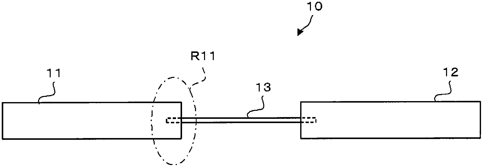
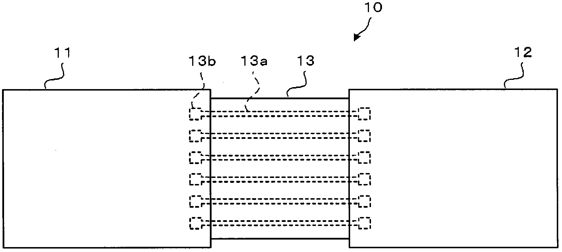
[0085] Such as Figure 1A as well as Figure 1B As shown, the flex-rigid circuit board 10 of this embodiment roughly includes a first rigid substrate 11, a second rigid substrate 12, and a flexible substrate 13, and the first rigid substrate 11 and the second rigid substrate 12 face each other via the flexible substrate 13. ground configuration. In detail, the first rigid substrate 11 and the second rigid substrate 12 are arranged in the horizontal direction of the flexible substrate 13 .
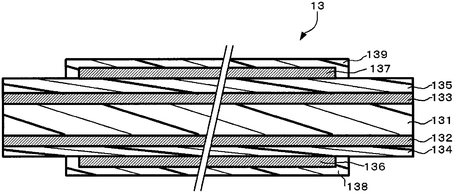
[0086] Arbitrary circuit patterns are formed on the first rigid substrate 11 and the second rigid substrate 12 , respectively. Moreover, electronic components, such as a semiconductor chip, etc. are connected as needed. On the other hand, strip-shaped wiring patterns 13 a for connecting the circuit patterns of the first rigid substrate 11 and the c...
PUM
 Abstract
Description
Claims
Application Information
 - Generate Ideas
- Intellectual Property
- Life Sciences
- Materials
- Tech Scout
- Unparalleled Data Quality
- Higher Quality Content
- 60% Fewer Hallucinations
Browse by: Latest US Patents, China's latest patents, Technical Efficacy Thesaurus, Application Domain, Technology Topic, Popular Technical Reports.
© 2025 PatSnap. All rights reserved.Legal|Privacy policy|Modern Slavery Act Transparency Statement|Sitemap|About US| Contact US: help@patsnap.com