
soi CMOS radio frequency switch, its forming method, and device using it

A radio frequency switch and device technology, applied to the device using the SOI CMOS radio frequency switch, the SOI CMOS radio frequency switch and the field of its formation, can solve problems such as signal loss of the SOI CMOS radio frequency switch, achieve no nonlinear effect, and reduce the amount of loss , easy to achieve effect

Active Publication Date: 2011-12-21
SHANGHAI HUAHONG GRACE SEMICON MFG CORP
View PDF5 Cites 11 Cited by
  • Summary
  • Abstract
  • Description
  • Claims
  • Application Information

AI Technical Summary

Problems solved by technology

Embodiments of the present invention can solve the problem of SOI CMOS RF switch signal loss and nonlinear effects

Method used


Image

  • soi CMOS radio frequency switch, its forming method, and device using it
  • soi CMOS radio frequency switch, its forming method, and device using it
  • soi CMOS radio frequency switch, its forming method, and device using it

Examples


Embodiment Construction

[0026] It can be seen from the background art that the existing SOI CMOS radio frequency switch will cause signal loss and non-linear effects.

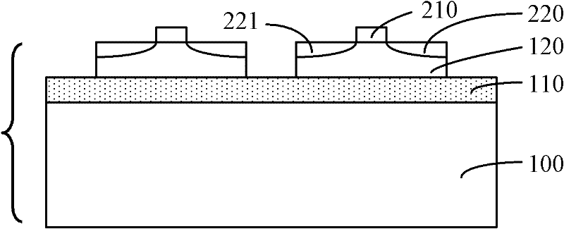
[0027] The inventor studies the above-mentioned problems and finds that the signal loss caused by the SOI CMOS radio frequency switch is caused by the high resistivity single crystal silicon support substrate 100 of the SOI substrate (for details, refer to figure 1 ).

[0028] Specifically, please refer to figure 2 , figure 2 It is a schematic diagram of current relationship among transistors in an existing SOI CMOS radio frequency switch. Such as figure 2 As shown, the SOI CMOS RF switch contains n transistors in series, and the current is transmitted sequentially along the order of the first transistor, the second transistor...the nth transistor as an example. During the current transmission process, Part of the current flows to the gate, and part of the current flows to the substrate, so for the nth transistor:

[0029] ID ...


PUM


Abstract

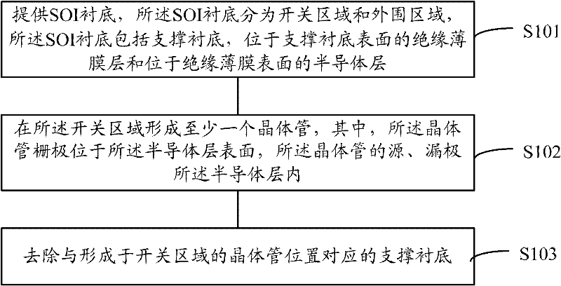
A method for forming a SOI CMOS radio frequency switch, an SOI CMOS radio frequency switch formed by the method, and a device using the SOI CMOS radio frequency switch formed by the method, the method for forming the SOICMOS radio frequency switch includes providing an SOI substrate, The SOI substrate is divided into a switch area and a peripheral area, and the SOI substrate includes a supporting substrate, an insulating film layer and a semiconductor layer formed in sequence; at least one transistor is formed in the switch area, wherein the transistor gate Located on the surface of the semiconductor layer, the source and drain of the transistor are inside the semiconductor layer; the supporting substrate corresponding to the position of the transistor formed in the switch region I is removed. The invention can avoid the signal loss problem and nonlinear effect of the existing SOI CMOS radio frequency switch.

Description

technical field [0001] Embodiments of the present invention relate to system chip technology, in particular to an SOI CMOS radio frequency switch and its forming method, and a device using the SOI CMOS radio frequency switch. Background technique [0002] With the continuous development of wireless communication technology, there is a situation where multiple communication standards coexist, such as GSM, WCDMA, CDMA, TD-SCDMA and so on. In order to make the same wireless communication mobile phone terminal available all over the world, it is required that the mobile phone terminal must support these different communication standards at the same time. Therefore, multiple radio frequency power amplifiers supporting different communication standards are required in the mobile terminal, and a radio frequency switch is used to switch the required radio frequency power amplifiers to the transmission channel. At the same time, radio frequency switches can also be used to switch tr...

Claims


Application Information

Patent Timeline
IPC IPC(8): H01L21/84H01L27/12H03K17/687
Inventor 许丹
Owner SHANGHAI HUAHONG GRACE SEMICON MFG CORP
Learn More