
Adaptive parametric power amplifier protection circuit

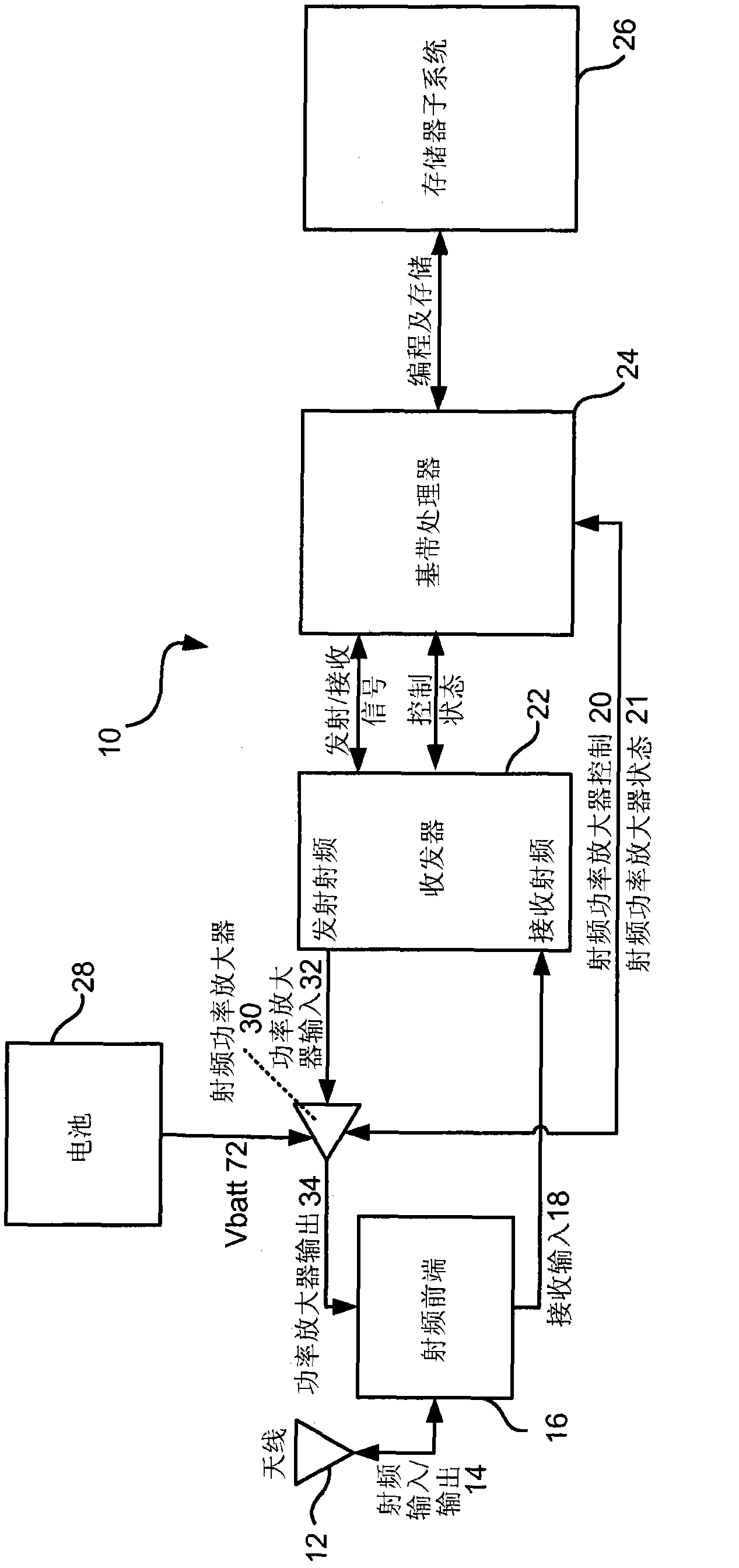
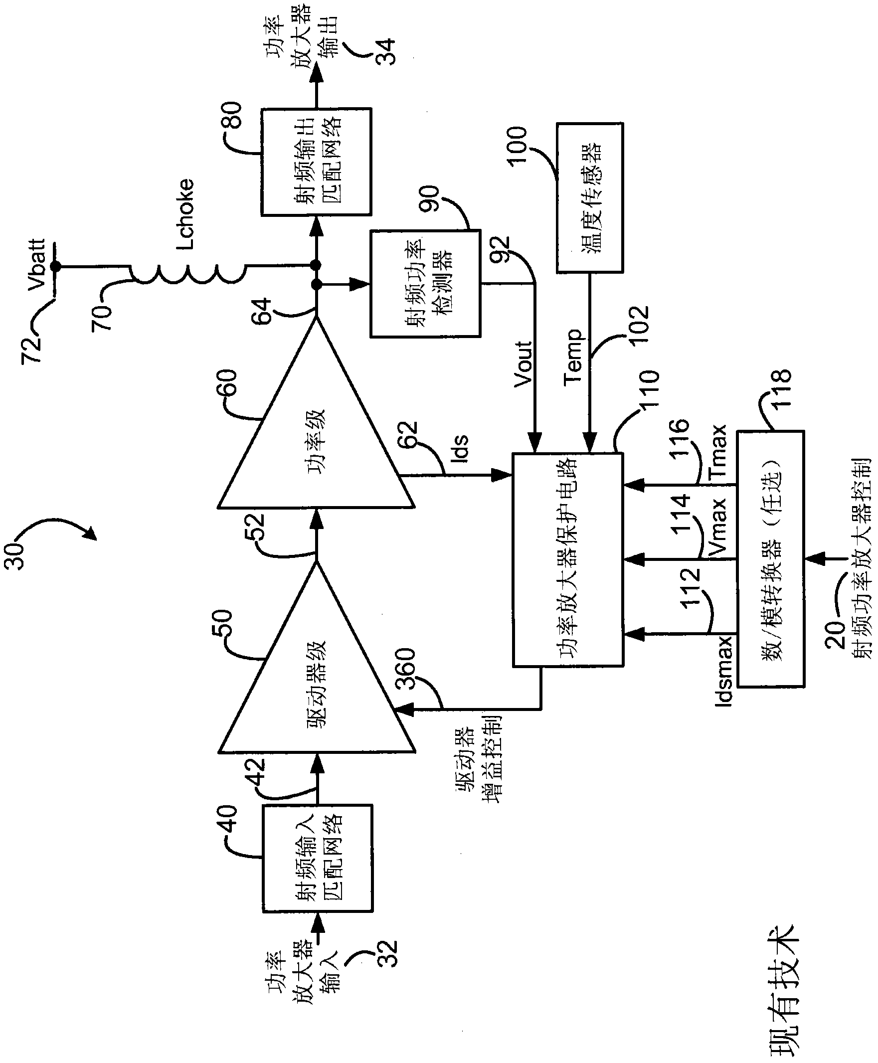
A protection circuit, self-adaptive technology, applied in the layout of amplifier protection circuit, power amplifier, amplifier, etc., can solve the problems of power amplifier circuit output voltage increase, top transistor drain-to-gate voltage damage, etc.

Inactive Publication Date: 2012-05-02
QUALCOMM INC
View PDF7 Cites 7 Cited by
  • Summary
  • Abstract
  • Description
  • Claims
  • Application Information

AI Technical Summary

Problems solved by technology

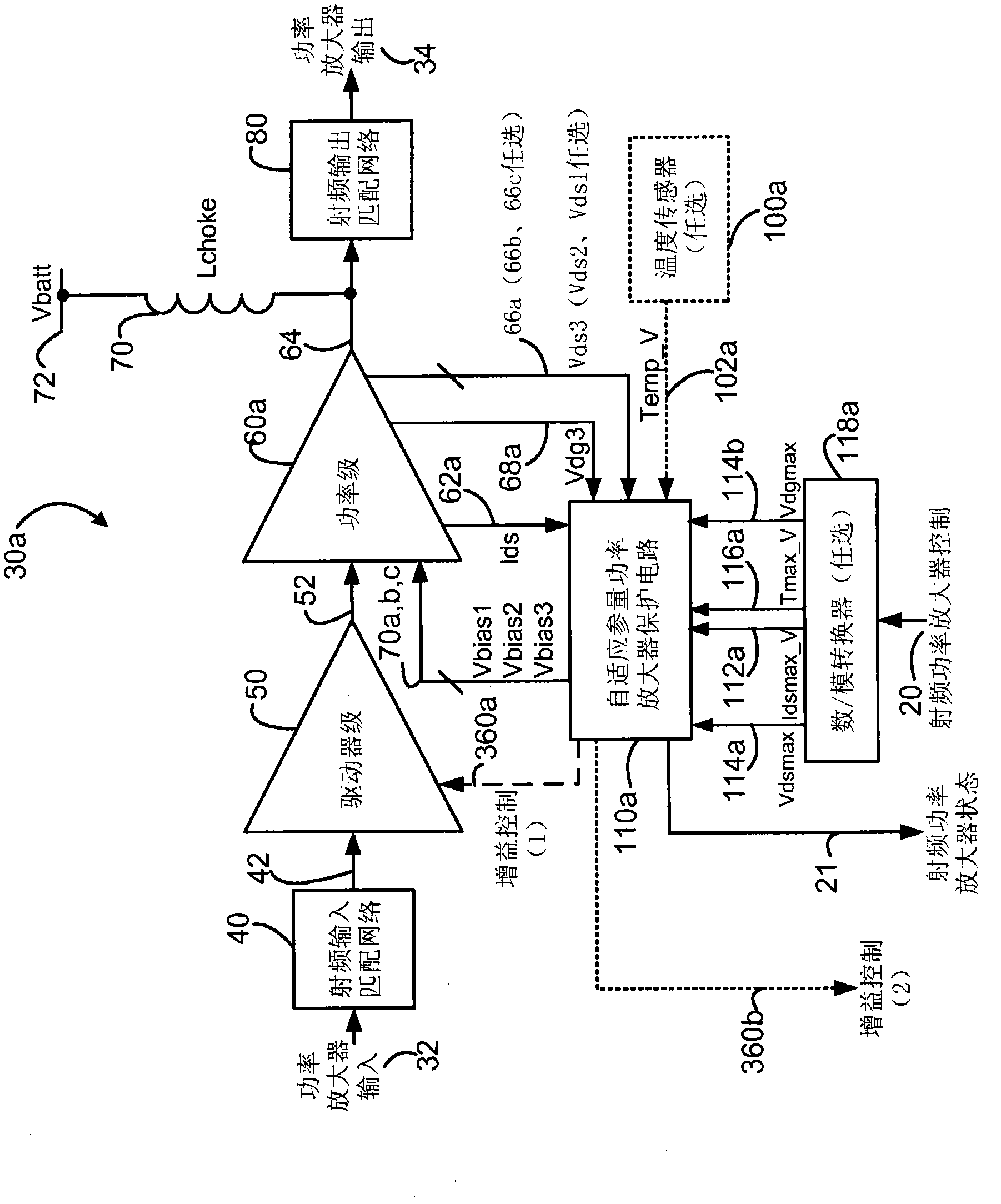
While this prevents each transistor from reaching its breakdown voltage, the drain-to-gate voltage of the top transistor can cause damage when the output voltage peaks
Furthermore, if the output of the power amplifier circuit is attached to an antenna, a change in the voltage standing wave ratio (VSWR) of the antenna may cause the output voltage of the power amplifier circuit to increase to even greater voltage levels

Method used


Image

  • Adaptive parametric power amplifier protection circuit
  • Adaptive parametric power amplifier protection circuit
  • Adaptive parametric power amplifier protection circuit

Examples


Embodiment Construction

[0010] The word "exemplary" is used herein to mean "serving as an example, instance, or illustration." Any embodiment described herein as "exemplary" is not necessarily to be construed as preferred or advantageous over other embodiments.

[0011] The detailed description set forth below in connection with the accompanying drawings is intended as a description of exemplary embodiments of the invention and is not intended to represent the only embodiments in which the invention may be practiced. The term "exemplary" is used throughout this description to mean "serving as an example, instance, or illustration" and is not necessarily to be construed as preferred or advantageous over other exemplary embodiments. The detailed description includes specific details for the purpose of providing a thorough understanding of exemplary embodiments of the invention. It will be readily apparent to those skilled in the art that the exemplary embodiments of the invention may be practiced with...


PUM


Abstract

A device including a gain control element coupled prior to or within a radio frequency (RF) power amplifier (PA) with an adaptive parametric PA protection circuit is described. In an exemplary embodiment, the device includes a gain control element coupled prior to a radio frequency power amplifier with a power stage with corresponding transistor breakdown threshold values, having an adaptive parametric PA protection circuit configured to receive at least one power stage drain-source voltage parameter value, at least one power stage drain-gate voltage parameter value, and at least one power stage drain-source current parameter value, and the device includes an adaptive parametric PA protection circuit having a first section for processing the parameter values and a second section for generating a gain correction signal to adjust the gain control element with optimal power added efficiency (PAE)for the power stage within the corresponding transistor breakdown threshold values.

Description

technical field [0001] The present invention relates generally to electronic devices and, more particularly, to adaptive parametric power amplifier protection circuits. Background technique [0002] In communication devices designed to transmit signals, such as cellular devices, power amplifier circuits are typically used to amplify the desired signal to allow proper transmission. For example, power amplifier circuits may be implemented in complementary metal oxide semiconductor (CMOS) technology or bipolar junction transistor (BJT) technology. For example, a power amplifier circuit may include two or more cascaded gain stages, a driver stage, and a power stage. The power stage may include CMOS transistors or BJT transistors. Both CMOS transistors and BJT transistors have breakdown voltages which, if exceeded, can lead to transistor damage. The breakdown voltage is the maximum voltage which, when applied across any two terminals of a transistor, can cause damage to the tr...

Claims


Application Information

Patent Timeline
IPC IPC(8): H04B1/04H03F1/52
CPCH03F1/523H03F2200/468H04B1/0466H03F3/24H03F2200/447H03F1/52H04B1/04
Inventor 阿里斯托泰莱·哈奇克里斯托斯居尔卡瓦·S·萨霍塔
Owner QUALCOMM INC
Learn More