Non-volatile memory compatible with complementary metal oxide semiconductor (CMOS) logical process and preparation method for non-volatile memory
A non-volatile, memory technology, applied in semiconductor/solid-state device manufacturing, electrical solid-state devices, semiconductor devices, etc., can solve problems such as expensive, small chip size, and complexity, and achieve compact structure, improved adaptability, and reduced processing cost effect
- Summary
- Abstract
- Description
- Claims
- Application Information
AI Technical Summary
Problems solved by technology
Method used
Image

Examples
Embodiment Construction
[0050] The present invention will be further described below in conjunction with specific drawings and embodiments.
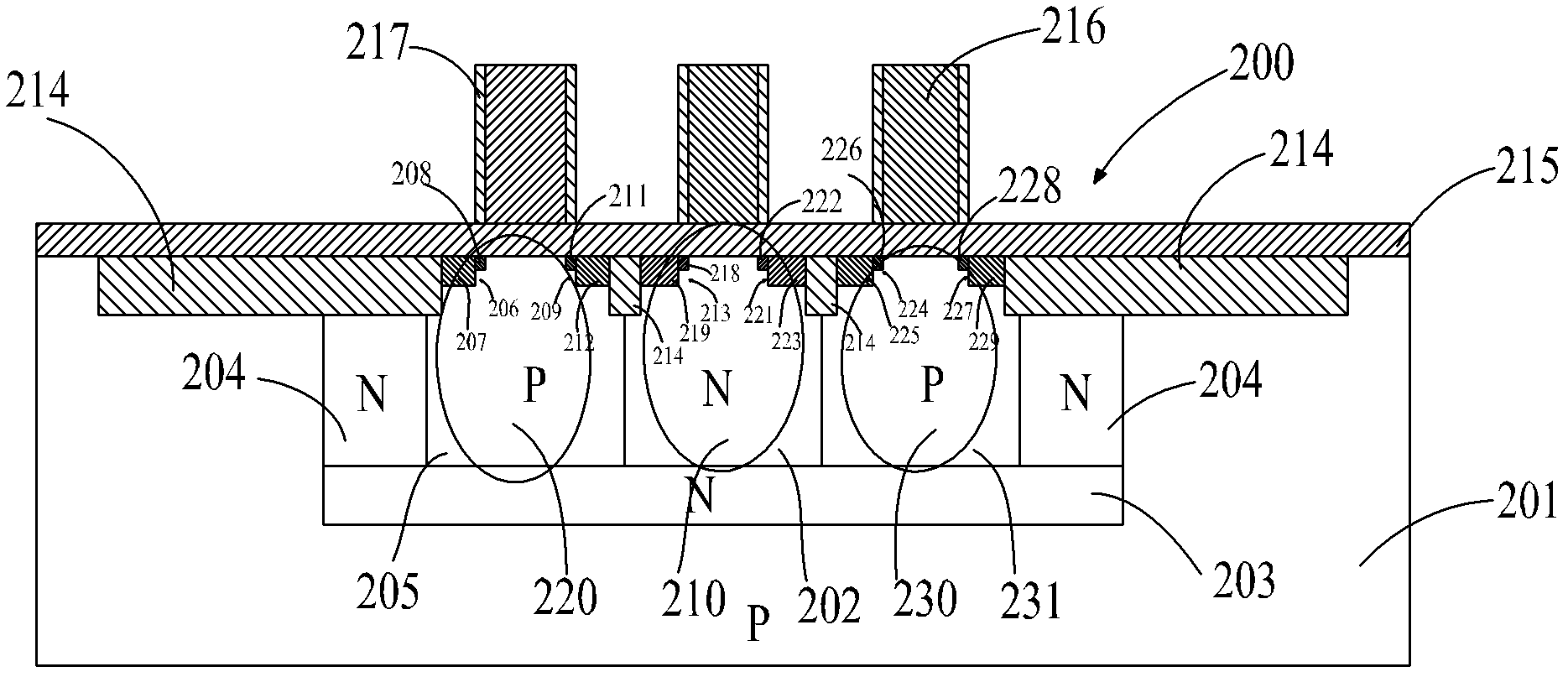
[0051] like figure 1 As shown: in order to make the non-volatile memory compatible with the CMOS logic process, the non-volatile memory includes a semiconductor substrate 201, the semiconductor substrate 201 is a substrate of P conductivity type, and the material of the semiconductor substrate 201 is silicon. The upper part of the semiconductor substrate 201 is provided with at least one memory cell 200, the memory cell 200 includes an access transistor, an NMOS control capacitor 220 and an NMOS programming transistor 230, and a gate dielectric layer 215 is deposited on the surface of the semiconductor substrate 201, The gate dielectric layer 215 covers the surface corresponding to the memory cell 200 , and the access transistor, the NMOS control capacitor 220 and the NMOS programming transistor 230 are isolated from each other by the domain dielectric region 2...
PUM
 Abstract
Description
Claims
Application Information
 - R&D Engineer
- R&D Manager
- IP Professional
- Industry Leading Data Capabilities
- Powerful AI technology
- Patent DNA Extraction
Browse by: Latest US Patents, China's latest patents, Technical Efficacy Thesaurus, Application Domain, Technology Topic.
© 2024 PatSnap. All rights reserved.Legal|Privacy policy|Modern Slavery Act Transparency Statement|Sitemap