Liquid crystal display device
A liquid crystal display device, liquid crystal technology, applied in static indicators, nonlinear optics, instruments, etc., can solve problems such as uneven display
- Summary
- Abstract
- Description
- Claims
- Application Information
AI Technical Summary
Problems solved by technology
Method used
Image

Examples
Embodiment 1
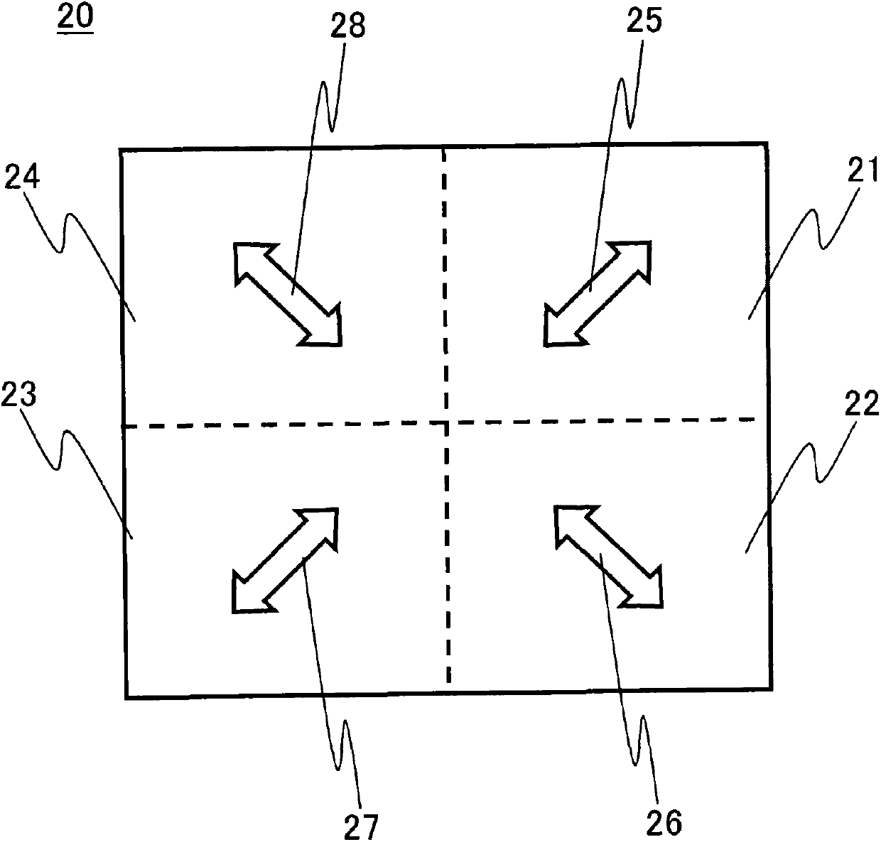
[0143] The liquid crystal display device of Example 1 was produced by applying the above-described liquid crystal 2 to the vertical alignment type liquid crystal display device capable of multiplexing of the present embodiment. Assuming that the electrode structure of the pixel of the liquid crystal display device of Example 1 is the same as Figure 10 The illustrated first example of the second electrode method applicable to the vertical alignment type liquid crystal display device of the present embodiment is the same. In this case, the size of one pixel is set to 0.39 mm square, the formation pitch of sub-pixels is set to 80 μm, and the width of the linear cutouts is set to 10 μm. Panel resistivity is 4.6×10 10 Ωcm. It is known that using the vertical alignment type liquid crystal display device of Example 1, the time from the application of static electricity to the substrate surface displaying the liquid crystal layer to the elimination of the charging is 5 seconds, whi...
Embodiment 2
[0146] The liquid crystal display device of Example 2 was manufactured by applying the above-described liquid crystal 2 to the vertical alignment type liquid crystal display device capable of multiplexing of the present embodiment. Assuming that the electrode structure of the pixel of the liquid crystal display device of Example 2 is the same as Image 6 The illustrated first example of the first electrode method applicable to the vertical alignment type liquid crystal display device of the present embodiment is the same. In this case, the size of one pixel was set to 0.39 mm square, the formation pitch of sub-pixels was set to 80 μm, and the widths of the linearly extending cutout portions of the curved cutouts were all set to 10 μm. Panel resistivity is 4.6×10 10 Ωcm.
[0147] It is known that using the vertical alignment type liquid crystal display device of Example 2, the time from the application of static electricity to the substrate surface displaying the liquid cryst...
Embodiment 3
[0150] The liquid crystal display device of Example 3 was produced by applying the above-described liquid crystal 2 to the vertical alignment type liquid crystal display device capable of multiplexing of the present embodiment. Assuming that the electrode structure of the pixel of the liquid crystal display device of Example 3 is the same as Figure 11 The illustrated second example of the second electrode method applicable to the vertical alignment type liquid crystal display device of the present embodiment is the same. In this case, the size of one pixel is set to 0.39 mm square, the formation pitch of sub-pixels is set to 80 μm, and the width of the linear cutouts is set to 10 μm. Panel resistivity is 4.6×10 10 Ωcm. It is known that using the vertical alignment type liquid crystal display device of Example 3, the time from the application of static electricity to the substrate surface displaying the liquid crystal layer to the elimination of the electrification is 5 seco...
PUM
| Property | Measurement | Unit |
|---|---|---|
| refractive index | aaaaa | aaaaa |
Abstract
Description
Claims
Application Information
 - R&D
- Intellectual Property
- Life Sciences
- Materials
- Tech Scout
- Unparalleled Data Quality
- Higher Quality Content
- 60% Fewer Hallucinations
Browse by: Latest US Patents, China's latest patents, Technical Efficacy Thesaurus, Application Domain, Technology Topic, Popular Technical Reports.
© 2025 PatSnap. All rights reserved.Legal|Privacy policy|Modern Slavery Act Transparency Statement|Sitemap|About US| Contact US: help@patsnap.com