Check patentability & draft patents in minutes with Patsnap Eureka AI!

Silicon carbide semiconductor device and manufacturing method of the same

A manufacturing method and technology of silicon carbide, applied in semiconductor/solid-state device manufacturing, semiconductor devices, electrical components, etc., can solve problems such as difficulty in forming trench sidewalls

Active Publication Date: 2015-01-28
DENSO CORP +1
View PDF6 Cites 0 Cited by
  • Summary
  • Abstract
  • Description
  • Claims
  • Application Information

AI Technical Summary

Problems solved by technology

Therefore, it is difficult to form trench sidewalls precisely parallel to the (11-20) plane

Method used


Image

  • Silicon carbide semiconductor device and manufacturing method of the same
  • Silicon carbide semiconductor device and manufacturing method of the same
  • Silicon carbide semiconductor device and manufacturing method of the same

Examples


no. 1 example

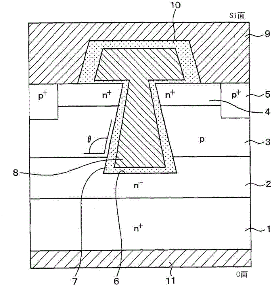
[0022] will refer to figure 1 A SiC semiconductor device according to a first embodiment of the present disclosure is described. SiC semiconductor devices include vertical MOSFETs with trench gate structures. In this embodiment, for example, the first conductivity type is set as n-type, and the second conductivity type is set as p-type.

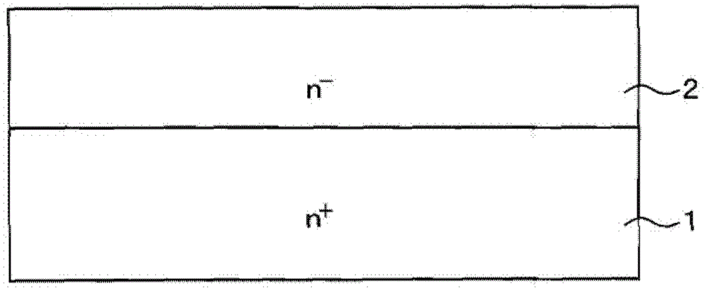
[0023] like figure 1 shown, using SiC made n + type substrate 1 to fabricate vertical MOSFETs. no + The substrate 1 has a Si plane as a main surface, which is a (0001) Si plane. no + Type substrate 1 is doped with a concentration of, for example, 1.0×10 19 / cm 3 n-type impurity, such as phosphorus, and has a thickness of about 300 μm. in n + type substrate 1 is formed on the surface of SiC made of n - Type drift layer 2. no - Type drift layer 2 is doped with a concentration of, for example, 5.0×10 15 / cm 3 to 2.0×10 16 / cm 3 n-type impurity, such as phosphorus, and has a thickness of about 8 μm to 15 μm. in n - A p-type bas...

no. 2 example

[0046] A SiC semiconductor device according to a second embodiment of the present disclosure will be described. Since in this embodiment, the shape of the groove 6 is changed from that of the first embodiment and otherwise similar to the first embodiment, only the different parts will be described.

[0047] like Figure 4 As shown, in this embodiment, the corners of the bottom of the trench 6 are rounded. The SiC semiconductor device according to this embodiment can basically be manufactured using the manufacturing method described in the first embodiment. allowable Figure 3A In the manufacturing process shown, the rounding of the bottom corners of the trench 6 is performed by controlling the etching conditions during the formation of the trench 6 , or by performing sacrificial oxidation and heat treatment after the formation of the trench 6 .

[0048] In the SiC semiconductor device according to the present embodiment, when the sidewall of the p-type base region 3 forming...


PUM


Abstract

An SiC semiconductor device includes a substrate, a drift layer, a base region, a source region, a trench, a gate oxide film, a gate electrode, a source electrode and a drain electrode. The substrate has a Si-face as a main surface. The source region has the Si-face. The trench is provided from a surface of the source region to a portion deeper than the base region and extends longitudinally in one direction and has a Si-face bottom. The trench has an inverse tapered shape, which has a smaller width at an entrance portion than at a bottom, at least at a portion that is in contact with the base region.

Description

technical field [0001] The present invention relates to a silicon carbide (hereinafter referred to as SiC) semiconductor device in which a semiconductor element having a trench gate structure is formed. The invention also relates to a method for manufacturing a SiC semiconductor device. Background technique [0002] As conventionally known vertical semiconductor elements made of a SiC substrate and having a trench gate structure, JP-A-2009-188221 and JP-A-2009-289987 disclose vertical metal oxide semiconductor field effect transistors (MOSFETs) . In the vertical MOSFETs disclosed in JP-A-2009-188221 and JP-A-2009-289987, in order to reduce the on-state resistance in the vertical MOSFET, it is necessary to increase the channel mobility. The channel mobility of SiC depends on the planar orientation. Therefore, in a vertical MOSFET having a trench gate structure, the planar direction of the main surface of the SiC substrate and the planar direction of the trench sidewalls ar...

Claims


Application Information

Patent Timeline
Patent Type & Authority Patents(China)
IPC IPC(8): H01L29/423H01L29/78H01L21/336
CPCH01L29/045H01L29/7813H01L29/66068H01L29/7397H01L29/42368H01L29/1608H01L29/4236
Inventor 三村智博宫原真一朗高谷秀史杉本雅裕副岛成雅石川刚渡边行彦
Owner DENSO CORP
Features
  • R&D
  • Intellectual Property
  • Life Sciences
  • Materials
  • Tech Scout
  • Unparalleled Data Quality
  • Higher Quality Content
  • 60% Fewer Hallucinations
Learn More