Method and apparatus for retrieving a phase of a wavefield
A wave field and phase technology, applied in optics, instruments, discharge tubes, etc., can solve problems such as intolerance to radiation, and achieve the effect of increasing effectiveness and increasing sample damage
- Summary
- Abstract
- Description
- Claims
- Application Information
AI Technical Summary
Problems solved by technology
Method used
Image


Examples
example 1
[0171] Presents results obtained from wavefield measurements with softer edges and stronger phase variations.
[0172] Conventional CDI methods have difficulty in addressing this situation.
[0173] Use of wave field Figure 7 The images shown in (a) and (b) are generated. Will Figure 7 The intensity value of the image pixel of (a) is multiplied by the intensity value of the corresponding pixel of the Airy disk in order to define the magnitude of the wavefield. Combined with AiryBlade to provide a soft border to the image. Amplitude scaled to the range [0,1].
[0174] The corresponding value of the wavefield phase is scaled to the [0,2π] range using the phase Figure 7 (b) image to define. overlap in Figure 7 (b) The dotted circle on the image indicates the application of Figure 7 The corresponding position of the first zero-valued contour of the Airy disc in (a).
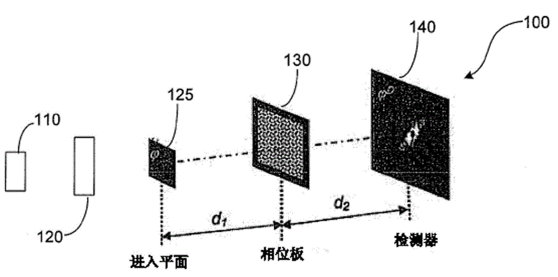
[0175] The setup parameters used for the algorithm are: λ=635 nm; d 1 =9.7 mm; d 2 =47.7 mm,...
example 2
[0207] The beam from the 635 nm laser diode is collimated and converged by a lens with a focal length of 50 mm to provide as Figure 5 The irradiation probe is shown. Place the WTD at a distance of approximately 18.45 mm behind the crossing point of the beam. WTDs are formed from silica glass etched into varying thicknesses in order to impart the desired phase retardation.
[0208] The WTD is formed to have 1100 x 1100 pixels, according to Figure 6 The examples shown are each square in shape and 16 μm wide. Each pixel is provided with a pinhole, whereby the pixel array provides a phase map. The pinholes have a hole size of 6 μm to minimize artifacts due to transition edges between pixels.
[0209] It will be appreciated that pinholes are not required, and arrangements that do not include pinholes are also useful.
[0210] A CCD camera with square pixels of 7.4 μm on each side was placed 70 mm downstream of the WTD in order to record the diffraction pattern.
[0211] Mic...
example 3
[0222] It is well known that phase recovery for one-dimensional (1D) signals is much more difficult than for higher-dimensional cases (2D or 3D), since the phase problem itself becomes more likely to be underdetermined. Restoring the phase of a one-dimensional signal has many applications, such as shape determination of ultrashort pulses and in geodesy, among others. This example proves that the method according to the embodiment of the present invention can also be applied to 1D signals through numerical experiments.
PUM
 Abstract
Description
Claims
Application Information
 - R&D
- Intellectual Property
- Life Sciences
- Materials
- Tech Scout
- Unparalleled Data Quality
- Higher Quality Content
- 60% Fewer Hallucinations
Browse by: Latest US Patents, China's latest patents, Technical Efficacy Thesaurus, Application Domain, Technology Topic, Popular Technical Reports.
© 2025 PatSnap. All rights reserved.Legal|Privacy policy|Modern Slavery Act Transparency Statement|Sitemap|About US| Contact US: help@patsnap.com