Method for preparing mixed solar cell based on reversal structure of GaN nanorods
The technology of a solar cell and its manufacturing method, which is applied in the field of microelectronics, can solve the problems of unfavorable large-scale application, low light transmittance, and high production cost, and achieve the effects of improving photoelectric conversion efficiency, high light transmittance, and reducing production cost
- Summary
- Abstract
- Description
- Claims
- Application Information
AI Technical Summary
Problems solved by technology
Method used
Image


Examples
Embodiment 1
[0030] Example 1: Making a hybrid solar cell with a nanocolumn height of 600nm and a pitch of 400nm:
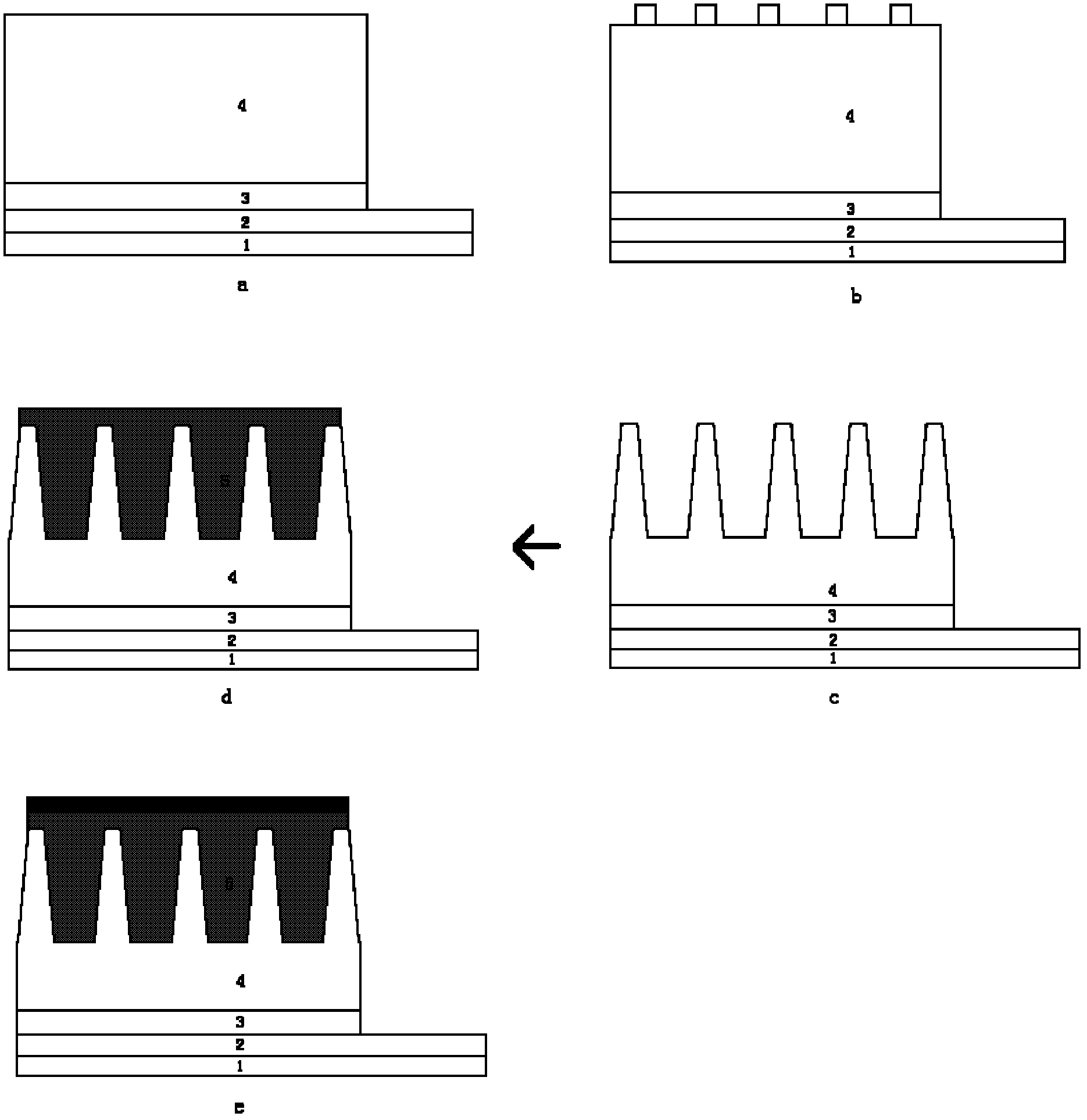
[0031] Step 1, using the ECR-PEMOCVD method to grow n-GaN layer on the indium tin oxide ITO conductive substrate, such as figure 2 a.
[0032] 1.1) Using hydrogen as the carrier gas and using high-purity nitrogen as the nitrogen source to grow a GaN buffer layer with a thickness of 75 nm on the indium tin oxide ITO, the growth process conditions are: nitrogen flow rate is 70 sccm, trimethylgallium flow rate is 0.4 sccm, The input microwave power is 650W, and the reaction temperature is 150°C;
[0033]1.2) Keep the gas flow rate, gas composition and microwave power constant, raise the substrate temperature to 350°C, and grow an n-GaN layer on the GaN buffer layer. The n-GaN layer has a thickness of 1.5 μm and a carrier concentration of 1×1017cm-3.
[0034] Step 2, put the indium tin oxide ITO conductive substrate grown with n-GaN into acetone, perform ultrasonic cleaning f...
Embodiment 2
[0044] Example 2: Making a hybrid solar cell with a nanocolumn height of 650nm and a pitch of 450nm:
[0045] Step 1, using the ECR-PEMOCVD method to grow n-GaN layer on the indium tin oxide ITO conductive substrate, such as figure 2 a.
[0046] First, using hydrogen as the carrier gas and high-purity nitrogen as the nitrogen source, the flow rate of nitrogen gas is 80 sccm, the flow rate of trimethylgallium is 0.5 sccm, the input microwave power is 600W, and the reaction temperature is 200°C. A GaN buffer layer with a thickness of 70nm is grown on tin ITO;
[0047] Then, keeping the gas flow rate, gas composition and microwave power constant, the substrate temperature was increased to 400°C, and the GaN buffer layer was grown with a thickness of 2 μm and a carrier concentration of 4×10 17 cm -3 n-GaN layer.
[0048] Step 2: Place the indium tin oxide ITO conductive substrate grown with n-GaN into acetone and absolute ethanol in sequence for ultrasonic cleaning for 2.5 mi...
Embodiment 3
[0059] Example 3: Making a hybrid solar cell with a nanocolumn height of 700nm and a spacing of 500nm:
[0060] Step A, using the ECR-PEMOCVD method to grow n-GaN layer on the indium tin oxide ITO conductive substrate, that is, first use hydrogen as the carrier gas, use high-purity nitrogen as the nitrogen source, and use the nitrogen flow rate as 90sccm, trimethylgallium The flow rate is 0.6sccm, the input microwave power is 700W, and the reaction temperature is 185°C, a GaN buffer layer with a thickness of 80nm is grown on the indium tin oxide ITO; The bottom temperature rises to 380°C, the thickness of the GaN buffer layer is 2.5 μm, and the carrier concentration is 1×10 18 cm -3 n-GaN layer, such as figure 2 a.
[0061] In step B, put the indium tin oxide ITO conductive substrate grown with n-GaN into acetone for 3 minutes for ultrasonic cleaning, then put it into absolute ethanol for 3 minutes, and finally rinse with deionized water for 15 minutes.
[0062] Step C, s...
PUM
 Abstract
Description
Claims
Application Information
 - R&D
- Intellectual Property
- Life Sciences
- Materials
- Tech Scout
- Unparalleled Data Quality
- Higher Quality Content
- 60% Fewer Hallucinations
Browse by: Latest US Patents, China's latest patents, Technical Efficacy Thesaurus, Application Domain, Technology Topic, Popular Technical Reports.
© 2025 PatSnap. All rights reserved.Legal|Privacy policy|Modern Slavery Act Transparency Statement|Sitemap|About US| Contact US: help@patsnap.com