

Array substrate, manufacturing method thereof and display device
An array substrate and a substrate technology are applied in the fields of array substrates and their manufacturing methods and display devices, and can solve problems such as over-etching, affecting product yield and the like
- Summary
- Abstract
- Description
- Claims
- Application Information
AI Technical Summary
Problems solved by technology
Method used
Image


Examples
Embodiment Construction
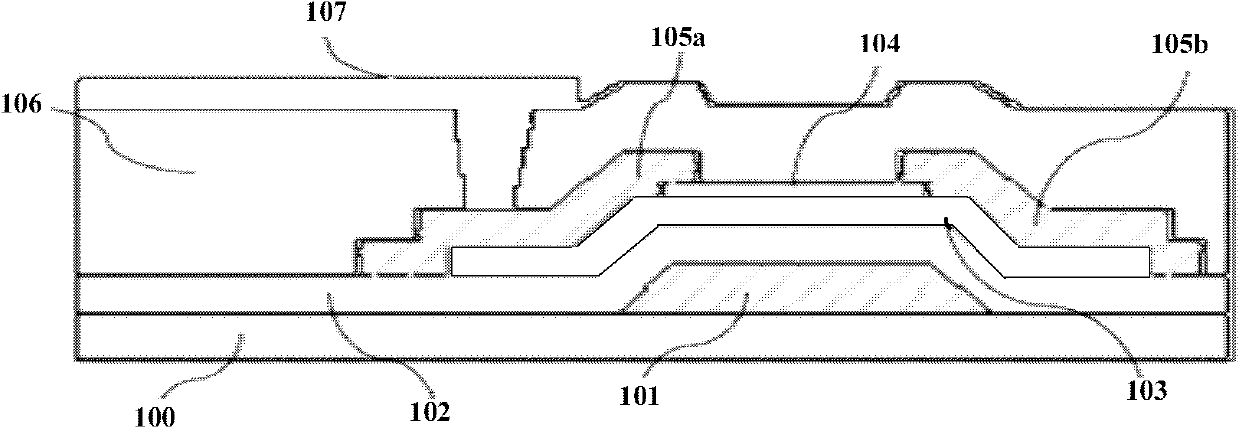
[0032] Embodiments of the present invention provide an array substrate, a manufacturing method thereof, and a display device. By improving the design of the etching barrier layer, the area of the etching barrier layer is greater than or equal to the area of the activation layer, and the area of the source electrode layer, the drain electrode layer and the activation layer are A through hole is provided at the junction of the layers, thereby avoiding additional step climbing when the source electrode layer, the drain electrode layer or the activation layer overlaps with the etching barrier layer.
[0033] Such as Figure 2a and Figure 2b As shown, the array substrate provided by the embodiment of the present invention includes:
[0034] Substrate 100, gate electrode layer 101, gate insulating layer 102, activation layer 103, etch barrier layer 104, source electrode layer 105a, drain electrode layer 105b, passivation layer 106 and transparent electrode layer 107, wherein...
PUM
 Abstract
Description
Claims
Application Information