
A kind of fabrication method of low temperature polysilicon thin film

A technology of low-temperature polysilicon and a manufacturing method, which is applied in semiconductor/solid-state device manufacturing, semiconductor devices, electrical components, etc., can solve problems such as large leakage current, influence on product quality, polysilicon film mobility and non-uniform threshold voltage, etc. Product quality, the effect of reducing leakage current

Inactive Publication Date: 2015-08-12
BOE TECH GRP CO LTD
View PDF5 Cites 0 Cited by
  • Summary
  • Abstract
  • Description
  • Claims
  • Application Information

AI Technical Summary

Problems solved by technology

[0004] Specifically, such as figure 1 As shown, a buffer layer 106 is formed on the substrate 101, and an amorphous silicon layer is formed on the buffer layer 106. After using ELA, the amorphous silicon layer is crystallized into a polysilicon layer 105, but the inventors have found that due to the ELA process Complicated, the amorphous silicon layer cannot be completely crystallized into a polysilicon layer, so that the surface of the formed polysilicon layer 105 is uneven and has many protrusions 104, so that when a voltage is applied to the thin film transistor, the protrusions on the surface of the polysilicon film will cause a tip discharge phenomenon , resulting in a large leakage current, and also due to the rough surface of the polysilicon film, resulting in a large resistance, making the mobility and threshold voltage of the polysilicon film uneven, affecting product quality

Method used


Image

  • A kind of fabrication method of low temperature polysilicon thin film
  • A kind of fabrication method of low temperature polysilicon thin film
  • A kind of fabrication method of low temperature polysilicon thin film

Examples


Embodiment Construction

[0020] The following will clearly and completely describe the technical solutions in the embodiments of the present invention with reference to the accompanying drawings in the embodiments of the present invention. Obviously, the described embodiments are only some, not all, embodiments of the present invention. Based on the embodiments of the present invention, all other embodiments obtained by persons of ordinary skill in the art without making creative efforts belong to the protection scope of the present invention.

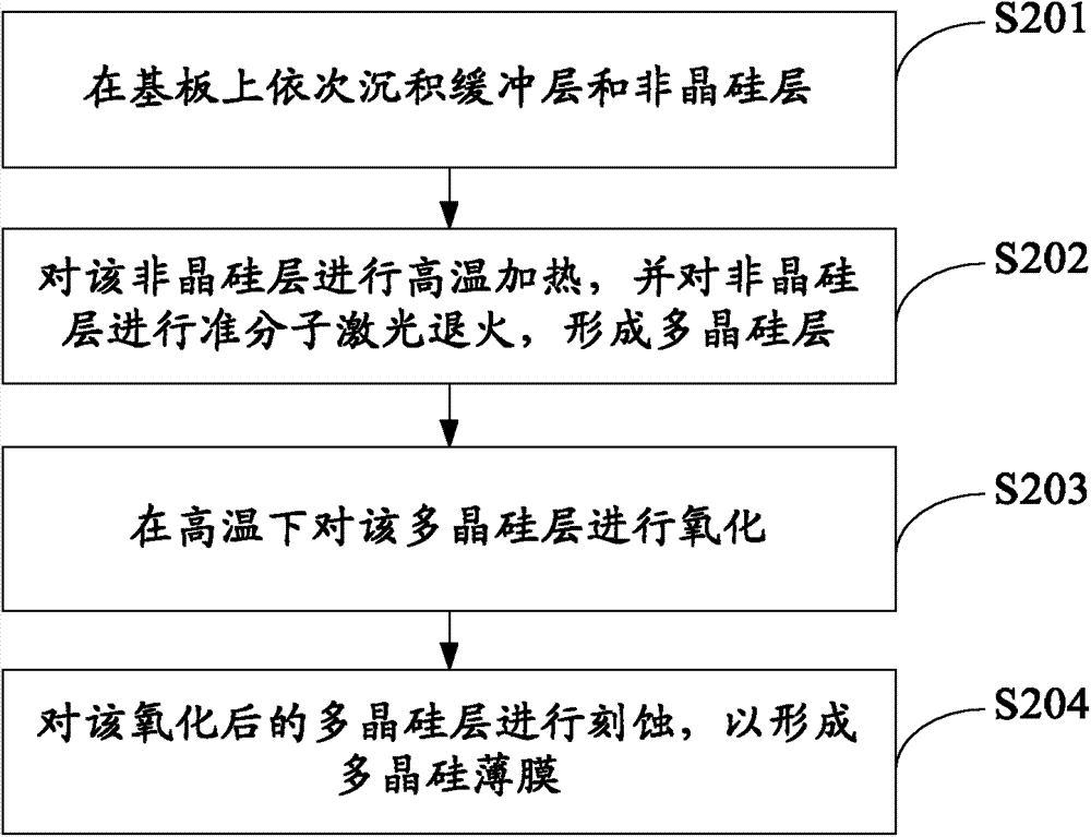
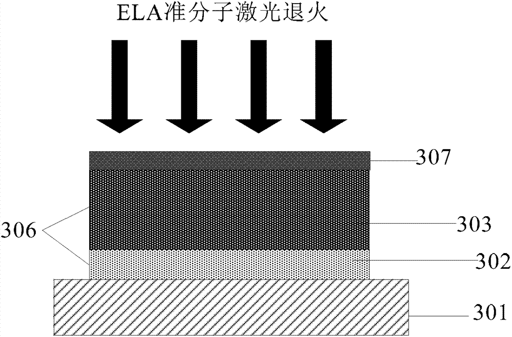
[0021] A method for manufacturing a low-temperature polysilicon thin film provided in an embodiment of the present invention, such as figure 2 shown, including:

[0022] S201, sequentially depositing a buffer layer and an amorphous silicon layer on a substrate.

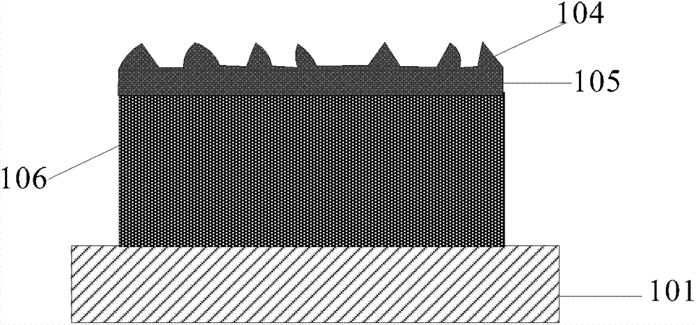
[0023] Specifically, such as image 3 As shown, a buffer layer 306 is deposited on the cleaned substrate 301, the buffer layer is composed of silicon nitride (SiN x ) layer 302 and silicon dioxide...


PUM

PropertyMeasurementUnit
thicknessaaaaaaaaaa
thicknessaaaaaaaaaa
thicknessaaaaaaaaaa

Abstract

Embodiments of the present invention provide a method for forming a low temperature polysilicon thin film. The method for forming the low temperature polysilicon thin film can comprise: depositing a buffer layer and an amorphous silicon layer on a substrate in this order; heating the amorphous silicon layer; performing an excimer laser annealing process on the amorphous silicon layer to form a polysilicon layer; oxidizing partially the polysilicon layer so as to form an oxidation portion at an upper portion of the polysilicon layer; and removing the oxidation portion of the polysilicon layer to form a polysilicon thin film.

Description

technical field [0001] The invention relates to the field of liquid crystal panel manufacture, in particular to a method for manufacturing a low-temperature polysilicon thin film. Background technique [0002] In the manufacturing process of the display, the formation of the polysilicon thin film of the active layer of the thin film transistor in the array substrate needs to be carried out at high temperature. Since the heat resistance of the general substrate is very low, if the polysilicon thin film is directly formed at high temperature, it will cause The substrate is deformed. Therefore, a low temperature polysilicon thin film (Low Temperature Polysilicon Thin Film) is usually used when making an active layer of a thin film transistor. [0003] Excimer Laser Annealing (Excimer Laser Annealing, can be abbreviated as ELA) method is currently the main method for producing low-temperature polysilicon thin films to achieve mass production. It uses high-energy excimer laser t...

Claims


Application Information

Patent Timeline
Patent Type & Authority Patents(China)
IPC IPC(8): H01L21/324H01L21/20
CPCH01L21/02686H01L21/02675H01L21/02532H01L21/02595H01L27/1285H01L21/32115H01L21/02664H01L21/02436
Inventor 田雪雁龙春平姚江峰
Owner BOE TECH GRP CO LTD
Learn More