Supercharge Your Innovation With Domain-Expert AI Agents!

Touch sensing element and conductive electrode structure

A technology of conductive electrodes and inductive elements, which is applied in the direction of electrical digital data processing, instruments, and input/output processes of data processing, etc., and can solve problems such as open circuit, inability to actuate, and large impedance

Active Publication Date: 2016-03-23
广州量子工业科技有限公司
View PDF7 Cites 0 Cited by
  • Summary
  • Abstract
  • Description
  • Claims
  • Application Information

AI Technical Summary

Problems solved by technology

[0008] The main problem of the current capacitive touch sensing element 1 is that the first conductive block 124, the second conductive block 125 and the connecting block 126 of the conductive structure 121 are made of transparent conductive materials, such as tin oxide or indium tin oxide, but transparent The surface resistance value per unit area of ​​the conductive material itself is about 30-100Ω / cm 2 , or even greater than 100Ω / cm 2 , so the equivalent circuit of the touch sensing element 1 will form a high impedance that is difficult to ignore, resulting in the larger the panel size, the larger the impedance, and even causing an open circuit and failing to operate

Method used


Image

  • Touch sensing element and conductive electrode structure
  • Touch sensing element and conductive electrode structure
  • Touch sensing element and conductive electrode structure

Examples


Embodiment Construction

[0047] The present invention will be described in detail below in conjunction with the accompanying drawings and embodiments.

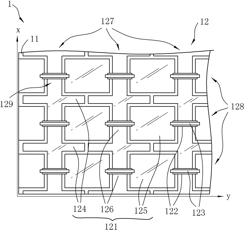
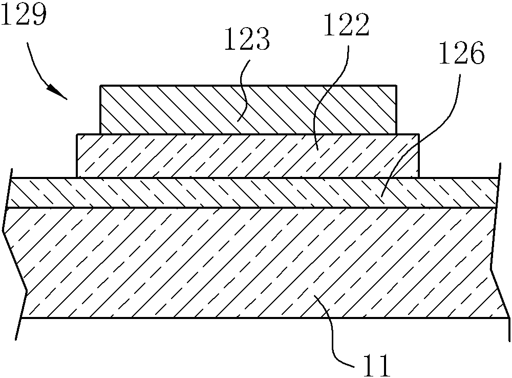
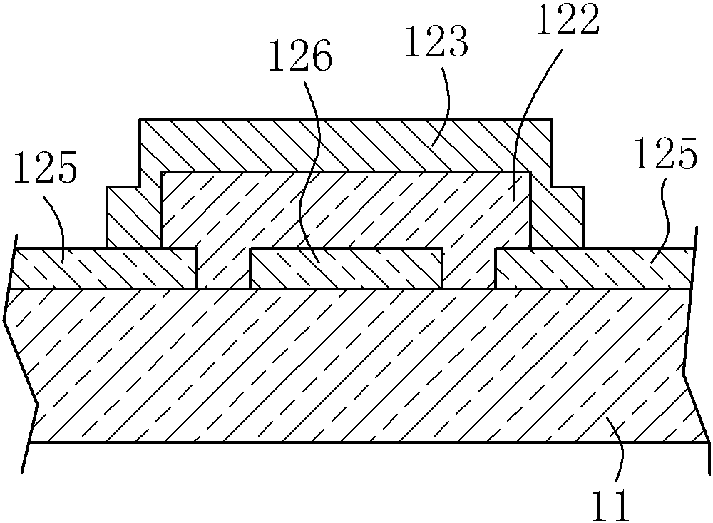
[0048] refer to Figure 4 , refer to Figure 5 , the first preferred embodiment of the present invention is illustrated by taking a capacitive touch sensing element 2 as an example, which includes a substrate 21 and a touch sensing circuit 22 disposed on the substrate 21 . The touch sensing circuit 22 includes a conductive block structure 221 , a conductive electrode structure 222 , and a plurality of dielectric films 223 .

[0049] The substrate 21 can be made of acrylic, polycarbonate, polyethylene, plastic, glass, and a combination thereof.

[0050] The conductive block structure 221 is made of conductive material and disposed on the substrate 21, and includes a plurality of first conductive blocks 224 arranged in an array and spaced apart from each other, and a plurality of second conductive blocks arranged in an array and spaced apart from each...


PUM


Abstract

A touch-type inductive device contains a substrate, a conductive block structure setting on the top of the substrate, a conductive electrode structure, and dielectric films, the conductive block structure contains the first conductive blocks and the second conductive blocks which are with arrayed arrangement, and connected blocks that connect the first conductive blocks as rows of the first conductive units, the conductive electrode structure contains the first conducting wires electrically connecting the first conductive blocks, the second conductive blocks electrically connect for each other as rows of the second conductive units, dielectric films are as separations at intersects with the first and second conductive units, the present invention uses the first conductive wires to reduce impedance, and applies to a large sized touch panel or to manufacture as a touch panel on a large sized substrate; the present invention also provides a conductive electrode structure that is suitable to apply to a large sized touch panel or to manufacture as a touch panel on a large sized substrate.

Description

technical field [0001] The invention relates to a sensing element, in particular to a touch sensing element and a conductive electrode structure. Background technique [0002] Touch technology was originally used in the field of industrial control. In recent years, the introduction of touch technology into panels of portable electronic products has become the mainstream of the market. There are mainly two types of touch panels: resistive touch panels and capacitive touch panels. Among them, the lifespan and tolerance of resistive touch panels are not enough, and they cannot continue to meet the stricter product specifications and stability required in the field of industrial control and consumer electronics in the future, while capacitive touch panels can also be applied to Multi-touch function, therefore, the capacitive touch panel has become the mainstream of touch panel development. [0003] refer to figure 1 , taking a capacitive touch sensing element 1 as an example ...

Claims


Application Information

Patent Timeline
Patent Type & Authority Patents(China)
IPC IPC(8): G06F3/041
Inventor 刘鸿达
Owner 广州量子工业科技有限公司
Features
  • R&D
  • Intellectual Property
  • Life Sciences
  • Materials
  • Tech Scout
  • Unparalleled Data Quality
  • Higher Quality Content
  • 60% Fewer Hallucinations
Learn More