UV-LIGA (Ultraviolet-Lithografie, Galvanoformung, Abformung) method for manufacturing multi layers of mini-type inductance coils on silicon substrate

A UV-LIGA and inductive coil technology, which is applied in the manufacture of circuits, electrical components, semiconductors/solid-state devices, etc., can solve the problems of affecting the electrical performance of coils, long production cycle of photographic substrates, and low cost performance, so as to improve production efficiency, Shorten the preparation period and design simple and convenient effects

Inactive Publication Date: 2012-10-10
DALIAN UNIV OF TECH
View PDF4 Cites 19 Cited by
  • Summary
  • Abstract
  • Description
  • Claims
  • Application Information

AI Technical Summary

Problems solved by technology

[0003] Helically wound inductance coils have certain disadvantages: for example, it is limited to the production of macroscopic inductance coils with a certain size, and it is powerless to produce microscopic inductance coils with a diameter of less than tens of microns; when the number of turns is large, the stability and mechanical strength of the coil structure are relatively low , prone to loosening, falling off, slipping, etc., which will affect the electrical properties of the coil, especially the hollow structure; it needs to be completed by personnel with certain operating experience
In the currently used technology, the first shortcoming is particularly obvious. At present, the sensor is developing in the dir

Method used


Image

  • UV-LIGA (Ultraviolet-Lithografie, Galvanoformung, Abformung) method for manufacturing multi layers of mini-type inductance coils on silicon substrate
  • UV-LIGA (Ultraviolet-Lithografie, Galvanoformung, Abformung) method for manufacturing multi layers of mini-type inductance coils on silicon substrate
  • UV-LIGA (Ultraviolet-Lithografie, Galvanoformung, Abformung) method for manufacturing multi layers of mini-type inductance coils on silicon substrate

Examples


Example Embodiment

[0030] Detailed description of the specific implementation of the present invention in conjunction with the drawings and technical solutions

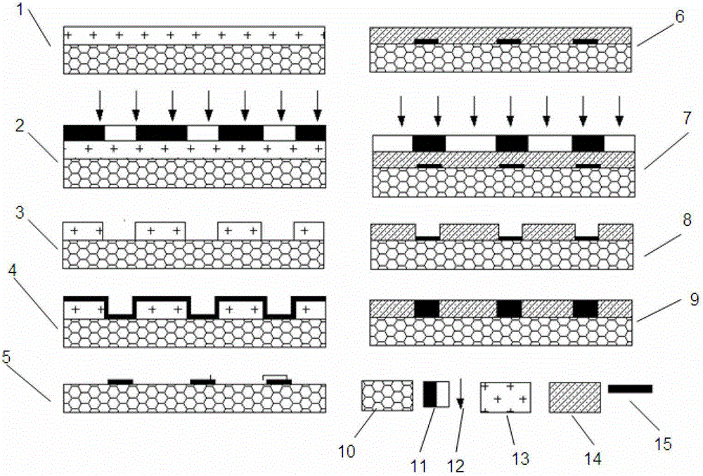
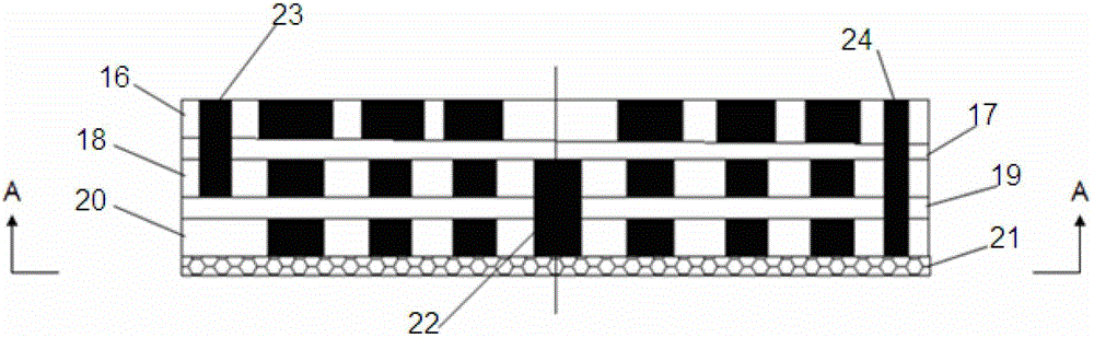
[0031] The process flow of the present invention is as follows figure 1 As shown, the specific steps are as follows:

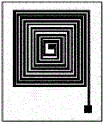
[0032] 1) Draw a mask pattern and make each layer of coil mask according to the designed inductor coil shape, size and layout. Choose a chromium plate. Each layer of coil needs a pattern (chromium in the shading area and no chromium in the light transmission area). The two negative masks are respectively used for the positive resist lithography in the sputtering stage and the negative resist lithography in the electroforming stage (the photosensitive characteristics of the positive and negative photoresist are opposite). The wire column between the coils and the insulating layer before the metal as the seed layer, so only the negative mask is needed for the negative photolithography in the electroforming stage;

[0033] 2) Ch...


PUM


Abstract

The invention discloses a UV-LIGA (Ultraviolet-Lithografie, Galvanoformung, Abformung) method for manufacturing multi layers of mini-type inductance coils on a silicon substrate. The UV-LIGA method integrates an MEMS (Micro Electro Mechanical System), a micro inductance coil of which the cross section diameter is ten micrometers and even several micrometers can be manufactured through a UV-LAIG craft of photoetching, developing, sputtering and electroforming craft and a PECVD (Plasma Enhanced Chemical Vapor Deposition) technology, and the size limit of the traditional manufacturing method of an inductance coil is broken. The UV-LIGA method disclosed by the invention is used for manufacturing a single-layer mini-type coil or multi layers of series-and-parallel communication structure coils, and the filling of insulation layers between the multi layers of the coils can be carried out through the PECVD technology. The bottom layer insulation effect is good as a silicon wafer is used as a substrate, the silicon wafer is light and the thin, and the operation is flexible; and a chromium plate is used as a masking tool, thus the transshipment from a design configuration to a manufacturing shape can be realized, the design for the size, the shape and the distribution of the inductance coil can be very flexible and simple, multiple sets of the inductance coils can be processed at one step according to the distribution of a masking configuration, the performance cost is high, and the processing efficiency and the forming rate are greatly increased.

Description

technical field [0001] The invention belongs to the technical field of inductance coil production, and in particular relates to a UV-LIGA process method for multilayer miniature inductance coils on a silicon substrate. Background technique [0002] At present, the manufacture of the inductance coil is either made by winding the paint leather wire along the insulated solenoid, or by the printed circuit board process. [0003] Helically wound inductance coils have certain disadvantages: for example, it is limited to the production of macroscopic inductance coils with a certain size, and it is powerless to produce microscopic inductance coils with a diameter of less than tens of microns; when the number of turns is large, the stability and mechanical strength of the coil structure are relatively low , prone to loosening, falling off, slipping and other phenomena that will affect the electrical properties of the coil, especially the hollow structure; it needs to be completed by ...

Claims


Application Information

Patent Timeline
IPC IPC(8): H01L21/02
Inventor 徐志祥姜凤娟寇锦尹嘉鹏
Owner DALIAN UNIV OF TECH
Why Eureka
Try Eureka