Supercharge Your Innovation With Domain-Expert AI Agents!

Semiconductor laser calibrating and testing method and application thereof

A test method and laser technology, applied in the field of optical communication, can solve the problems of laser tracking error, inaccurate calibration accuracy, not taking into account temperature gradient and environmental temperature changes, etc., so as to solve the tracking error and improve the calibration accuracy.

Active Publication Date: 2012-12-19
SUZHOU CREALIGHTS TECH
View PDF5 Cites 10 Cited by
  • Summary
  • Abstract
  • Description
  • Claims
  • Application Information

AI Technical Summary

Problems solved by technology

However, due to the difference in position and distance between the position of the internal temperature sensing device (such as a thermistor) and the position of the laser die, when the ambient temperature changes, there must be a temperature gradient between the temperature monitoring point and the laser die, resulting in a monitoring reference The temperature is inconsistent with the actual temperature of the laser die, and this temperature difference will change with the change of the external temperature, resulting in a deviation between the monitoring value used to report the system and the actual test value, resulting in a laser tracking error, thus causing damage to the laser module or use The module optical power of the laser monitors the accuracy and precision of DDM calibration, which brings uncertainty and error
[0004] The external calibration method currently used in the industry adopts two-point calibration by monitoring the back-facing photodetector inside the laser, and does not take into account the influence of temperature gradient and environmental temperature changes. Although the tracking error can be reduced, the calibration accuracy is not accurate. , cannot fundamentally solve the problem

Method used


Image

  • Semiconductor laser calibrating and testing method and application thereof
  • Semiconductor laser calibrating and testing method and application thereof
  • Semiconductor laser calibrating and testing method and application thereof

Examples


Embodiment Construction

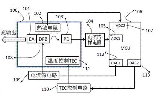
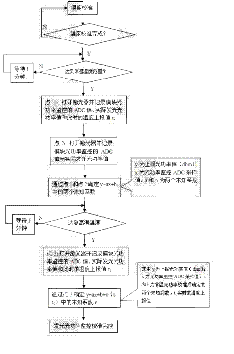
[0034] The calibration error of the semiconductor laser mainly comes from the temperature gradient of the internal die of the laser device and the temperature reference point, which directly affects the calibration of the optical power at the transmitting end, the optical wavelength of the wavelength division multiplexing (WDM) channel, and the optical power at the receiving end. Considering the commonality of these calibration methods, this article only discusses the calibration and monitoring of the luminous optical power.

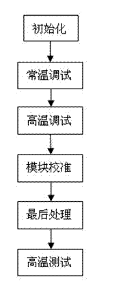
[0035] The following takes the EML laser with temperature control widely used in optical fiber communication as an example, and specifically introduces the testing method of the present invention. Of course, the method is also applicable to other semiconductor lasers.

[0036] Such as figure 1 As shown, consistent with the prior art, a semiconductor EML laser 100 with temperature control consists of an electroabsorption (EA) 101, a distributed reflective...


PUM


Abstract

The invention discloses a semiconductor laser calibrating and testing method. The semiconductor laser calibrating and testing method includes a step of debugging various parameters including input light power, output light power, extinction ratio, intersection, wavelength, the optimum sensitivity voltage, signal loss enabling energy and signal restoring enabling energy at the room temperature and high temperature, a step of calibrating a semiconductor laser module, a step of processing data, a step of high-temperature testing, and a step of detecting the semiconductor laser module. The step of calibrating the semiconductor laser module includes matching parameter values at states of turning on and off the semiconductor laser module at the room temperature, and matching relevant parameter values at the high temperature, and accordingly, obtaining relation between a monitoring value and a practical value. Meanwhile, the semiconductor laser calibrating and testing method can be applicable to calibrating testing of the semiconductor laser module. Affection on temperature gradient is sufficiently considered, tracking errors of a laser are solved, and calibrating accuracy of a semiconductor laser is effectively improved.

Description

technical field [0001] The present invention relates to a calibration test method of a semiconductor laser, in particular to a calibration test method based on an electroabsorption modulation semiconductor laser or a direct modulation digital monitoring part of a semiconductor laser module; at the same time, the method can also be applied to the calibration test of an optical module, It belongs to the field of optical communication. Background technique [0002] At present, semiconductor lasers, as key devices, have been widely used in the construction of optical fiber communication networks, and are used to load communication information onto optical signals and enter optical fibers for transmission. In order to obtain stable output power, wavelength and other laser characteristics, most semiconductor lasers need a built-in refrigerator to stabilize the core temperature of the laser. [0003] Theoretically, the temperature inside the laser tube core is controlled and const...

Claims


Application Information

Patent Timeline
Patent Type & Authority Applications(China)
IPC IPC(8): G01M11/00G01M11/02
Inventor 胡朝阳郑晓锋
Owner SUZHOU CREALIGHTS TECH
Features
  • R&D
  • Intellectual Property
  • Life Sciences
  • Materials
  • Tech Scout
  • Unparalleled Data Quality
  • Higher Quality Content
  • 60% Fewer Hallucinations
Learn More