Back-side contact formation
A back-contact and front-contact technology, applied in electrical components, electrical solid-state devices, circuits, etc., can solve the problems of die layout increasing production complexity and cost
- Summary
- Abstract
- Description
- Claims
- Application Information
AI Technical Summary
Problems solved by technology
Method used
Image

Examples
Embodiment Construction
[0013] Although the present disclosure can be modified into various modifications and alternative forms, examples of the present disclosure are shown by way of example in the drawings and will be described in detail. It should be understood, however, that the disclosure is not intended to be limited to the particular embodiments shown and / or described. On the contrary, the intention is to cover all modifications, equivalents, and alternatives falling within the spirit and scope of the disclosure.
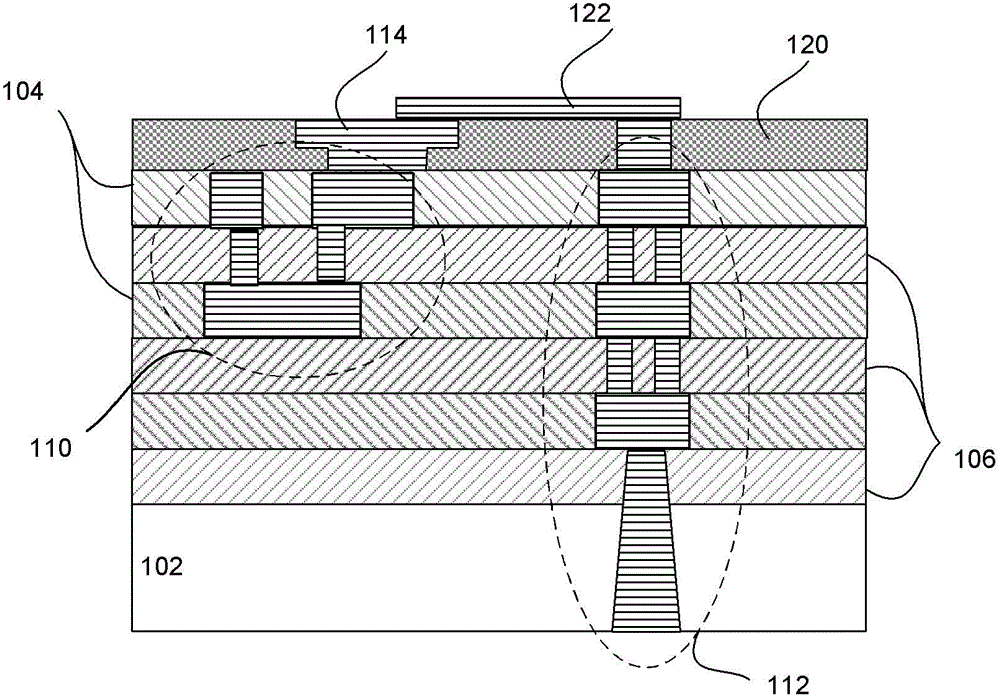
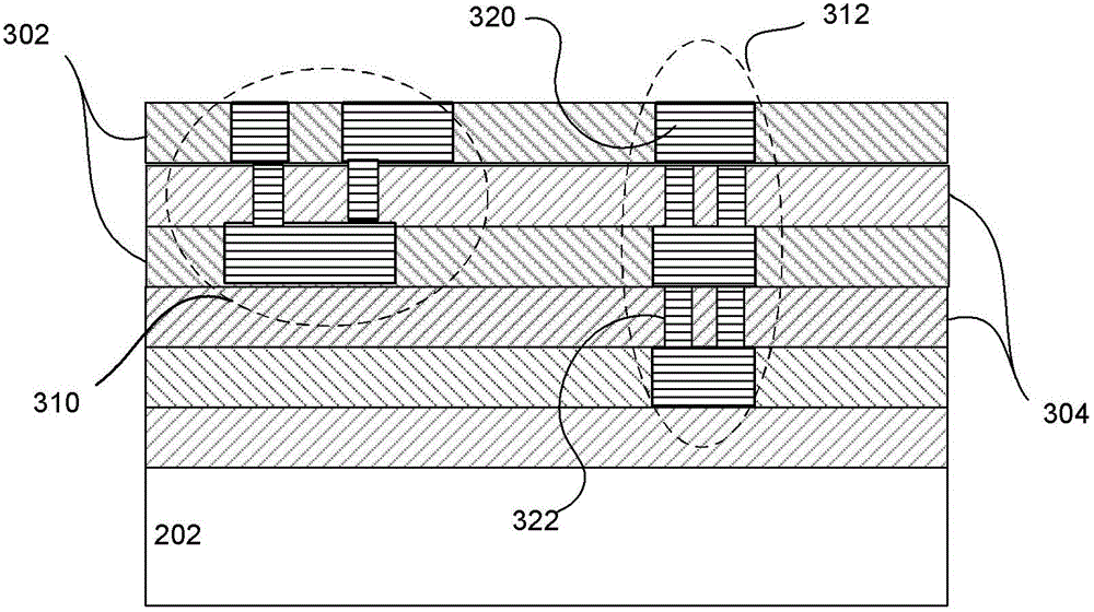
[0014] In one or more embodiments, a semiconductor die is provided that can be easily reconfigured by post-manufacturing processes to enable backside contacts. This capability allows a batch of the same semiconductor die to be used in a greater variety of applications. Some dies may be used in packages using front contact pads, while others may be used in packages using back contacts. Since this increases versatility and simplifies manufacturing, manufacturing costs can be reduced...
PUM
 Abstract
Description
Claims
Application Information
 - R&D
- Intellectual Property
- Life Sciences
- Materials
- Tech Scout
- Unparalleled Data Quality
- Higher Quality Content
- 60% Fewer Hallucinations
Browse by: Latest US Patents, China's latest patents, Technical Efficacy Thesaurus, Application Domain, Technology Topic, Popular Technical Reports.
© 2025 PatSnap. All rights reserved.Legal|Privacy policy|Modern Slavery Act Transparency Statement|Sitemap|About US| Contact US: help@patsnap.com