Supercharge Your Innovation With Domain-Expert AI Agents!

Electrostatic protection device and its chip

A technology for electrostatic protection and electrostatic discharge circuits, which can be used in circuits, electrical components, and electrical solid devices to solve problems such as increasing chip costs.

Active Publication Date: 2016-08-03
GUANGDONG YUEJING HIGH TECH CO LTD
View PDF5 Cites 0 Cited by
  • Summary
  • Abstract
  • Description
  • Claims
  • Application Information

AI Technical Summary

Problems solved by technology

Therefore, these capacitance and resistance elements on the chip will occupy a large area of ​​the chip used by the electrostatic protection device, thereby increasing the cost of the chip

Method used


Image

  • Electrostatic protection device and its chip

Examples


Embodiment Construction

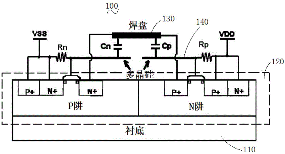
[0016] Please refer to figure 1 , an embodiment provides an electrostatic protection device 100 . The ESD protection device 100 includes a substrate 110 , an ESD protection component 120 formed on the substrate 110 providing an ESD circuit, and a pad 130 formed on the ESD protection component 120 . The ESD protection element 120 includes at least one resistor or capacitor. A polysilicon layer 140 is formed between the electrostatic protection element 120 and the pad 130 , and a dielectric layer (not shown in the figure) is formed between the pad 130 and the polysilicon layer 140 . At least one resistance or capacitance of the ESD protection element 120 is provided by the polysilicon layer 140 , the dielectric layer and the bonding pad 130 .

[0017] The polysilicon layer 140, the dielectric layer and the pad 130 can form a three-layer structure, wherein the polysilicon layer 140 and the pad 130 form two metal plates of the capacitor, and the dielectric layer forms the dielec...


PUM


Abstract

The invention provides an electrostatic protection device and a chip of the electrostatic protection device. The electrostatic protection device comprises a substrate, an electrostatic protection component and a bonding pad, wherein the electrostatic protection component is formed on the substrate and provides an electrostatic discharge circuit, and the bonding pad is formed on the electrostatic protection component. The electrostatic protection component comprises at least one resistor or capacitor. A polycrystalline silicon layer is formed between the electrostatic protection component and the bonding pad, and a dielectric layer is formed between the bonding pad and the polycrystalline silicon layer. Due to the fact that the at least one resistor or the capacitor formed among the polycrystalline silicon layer, the dielectric layer and the bonding pad are adopted to serve as the needed resistor and capacitor of the electrostatic protection device, the occupied area of the electrostatic protection device is reduced, and cost is saved.

Description

technical field [0001] The invention relates to a semiconductor device, in particular to an electrostatic protection device and a chip thereof. Background technique [0002] On the chip, the function of the electrostatic protection device is to prevent the semiconductor device on the chip from being damaged or invalidated by electrostatic discharge, thereby preventing the entire chip from being damaged or invalidated. Commonly used chips are generally equipped with an electrostatic protection device to prevent the chip from being damaged or invalidated by static electricity. ESD protection devices generally include components such as capacitors or resistors, and the values ​​of these capacitors and resistors are relatively large. Therefore, these capacitance and resistance elements on the chip will occupy a large area of ​​the chip where the electrostatic protection device is applied, thereby increasing the cost of the chip. Contents of the invention [0003] Based on th...

Claims


Application Information

Patent Timeline
Patent Type & Authority Patents(China)
IPC IPC(8): H01L23/60
Inventor 叶兆屏胥小平朱志牛沓世我张富启
Owner GUANGDONG YUEJING HIGH TECH CO LTD
Features
  • R&D
  • Intellectual Property
  • Life Sciences
  • Materials
  • Tech Scout
  • Unparalleled Data Quality
  • Higher Quality Content
  • 60% Fewer Hallucinations
Learn More