Check patentability & draft patents in minutes with Patsnap Eureka AI!

Signal sampling caching device used for field programmable gata array (FPGA) chip debugging

A signal sampling and caching technology, which is applied in memory systems, faulty computer hardware detection, memory address/allocation/relocation, etc., can solve problems such as limited storage depth, debugging logic insertion, and unsatisfactory timing, and achieve signal sampling The effect of large time span, high storage space utilization, and strong multi-signal sampling capability

Active Publication Date: 2015-07-22
NAT UNIV OF DEFENSE TECH
View PDF9 Cites 0 Cited by
  • Summary
  • Abstract
  • Description
  • Claims
  • Application Information

AI Technical Summary

Problems solved by technology

If the user's logic resources occupy a large amount and the timing requirements are strict, especially when the on-chip RAM usage is large, debugging tools such as ChipScope usually cannot be used normally. On the one hand, the resources are limited and the debugging logic that the user expects cannot be completed. Insertion; on the other hand, the increased debugging logic affects the layout and routing of user logic, and even fails due to timing failure
[0004] Although several major FPGA manufacturers have provided more convenient and functional internal signal observation tools, they are all limited by the very limited on-chip RAM resources inside the chip, and cannot meet the long-term requirements for internal signal observation. logic debug
If you use a high-end logic analyzer for signal sampling, on the one hand, it is expensive, and on the other hand, the storage depth is still very limited

Method used


Image

  • Signal sampling caching device used for field programmable gata array (FPGA) chip debugging
  • Signal sampling caching device used for field programmable gata array (FPGA) chip debugging
  • Signal sampling caching device used for field programmable gata array (FPGA) chip debugging

Examples


Embodiment Construction

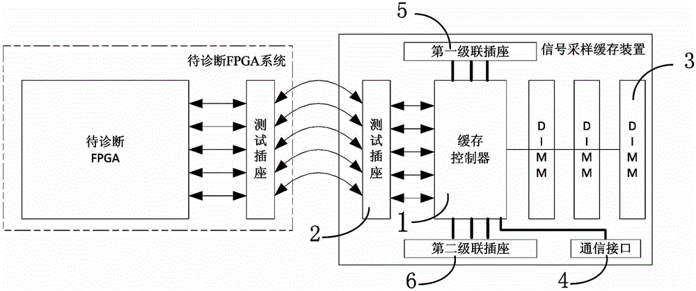
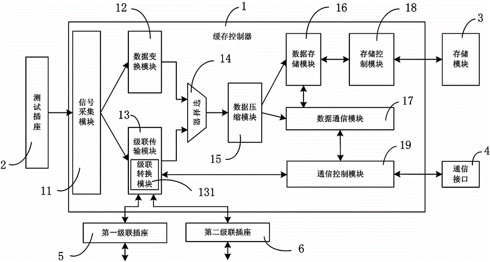
[0027] Such as figure 1 As shown, the signal sampling buffer device used for FPGA chip debugging in this embodiment includes a buffer controller 1, a test socket 2, a storage module 3, a communication interface 4 and a stage for realizing cascade connection between a plurality of signal sampling buffer devices The cascading socket module, the cache controller 1 is connected to the test socket 2, the storage module 3, and the communication interface 4 respectively, and the cascading socket module includes a signal sampling buffer device for connecting the upper level signal or the lower level signal respectively in the cascading working state. The first cascade socket 5 and the second cascade socket 6 of the sampling buffer device are connected to the cache controller 1 respectively. This embodiment aims at the problem that the internal signal observation and debugging tools provided by the existing FPGA manufacturers rely heavily on the scarce on-chip RAM resources inside the ...


PUM


Abstract

The invention discloses a signal sampling caching device used for field programmable gata array (FPGA) chip debugging. The signal sampling caching device used for FPGA chip debugging comprises a caching controller (1), a test plug seat (2), a storage module (3), a communication interface (4) and a cascading plug seat module used for achieving the cascade connection among a plurality of signal sampling caching devices. The caching controller (1) is respectively connected with the test plug seat (2), the storage module (3), and the communication interface (4). The cascading plug seat module comprises a first cascading plug seat (5) and a second cascading plug seat (6), wherein the first cascading plug seat (5) and the second cascading plug seat (6) are respectively used for being connected with a signal sampling caching device in an upper grade or a signal sampling caching device in a lower grade in a cascading working state. The first cascading plug seat (5) and the second cascading plug seat (6) are respectively connected with the caching controller (1). The signal sampling caching device used for FPGA chip debugging has the advantages of having no use for random access memory (RAM) resource in an FPGA chip and being high in usage ratio of storage space, large in signal sampling time span, strong in multiple signal sampling ability and flexible in usage method.

Description

technical field [0001] The invention relates to the field of logic debug (debugging) in FPGA applications, in particular to a signal sampling buffer device for FPGA chip debugging. Background technique [0002] As a reprogrammable logic array chip, FPGA is widely used in the design of prototype verification systems and batch products. User logic generates a corresponding bit stream through logic synthesis, resource mapping, and layout and routing processes through the design tools provided by the FPGA manufacturer. After the bit stream is imported into the FPGA chip, specific applications can be executed. Due to the advantages of flexible application and reprogrammable FPGA chips, the use of FPGA chips for prototype system design has become an important means of logic verification before most ASICs are put into production. [0003] FPGA chips, like ASIC chips, face the problems of difficulty in observing internal signals, which is not conducive to logic debugging. For this...

Claims


Application Information

Patent Timeline
Patent Type & Authority Patents(China)
IPC IPC(8): G06F12/08G06F11/25G06F12/0893
Inventor 张峻齐星云王桂彬常俊胜张建民罗章徐金波董德尊赖明澈陆平静王绍刚徐炜遐肖立权庞征斌王克非夏军童元满陈虎
Owner NAT UNIV OF DEFENSE TECH
Features
  • R&D
  • Intellectual Property
  • Life Sciences
  • Materials
  • Tech Scout
  • Unparalleled Data Quality
  • Higher Quality Content
  • 60% Fewer Hallucinations
Learn More