Supercharge Your Innovation With Domain-Expert AI Agents!

Display device, array substrate and manufacturing method thereof

A manufacturing method and technology of array substrates, which are applied in the photolithographic process of pattern surface, semiconductor/solid-state device manufacturing, optics, etc., can solve the problems of complex process, high cost, mask production capacity and yield limit, etc., and achieve the production process Simplicity and the effect of reducing manufacturing costs

Active Publication Date: 2015-11-11
BOE TECH GRP CO LTD
View PDF4 Cites 0 Cited by
  • Summary
  • Abstract
  • Description
  • Claims
  • Application Information

AI Technical Summary

Problems solved by technology

In the manufacturing process of TFT-LCD, the manufacturing cost of the mask is very expensive. Each formation of a structural layer requires only one mask with a specific pattern for exposure. The process is complicated and the cost is high. The production capacity and yield rate of each additional mask restricted

Method used


Image

  • Display device, array substrate and manufacturing method thereof
  • Display device, array substrate and manufacturing method thereof
  • Display device, array substrate and manufacturing method thereof

Examples


Embodiment Construction

[0044] The specific implementation manners of the present invention will be further described in detail below in conjunction with the accompanying drawings and embodiments. The following examples are used to illustrate the present invention, but are not intended to limit the scope of the present invention.

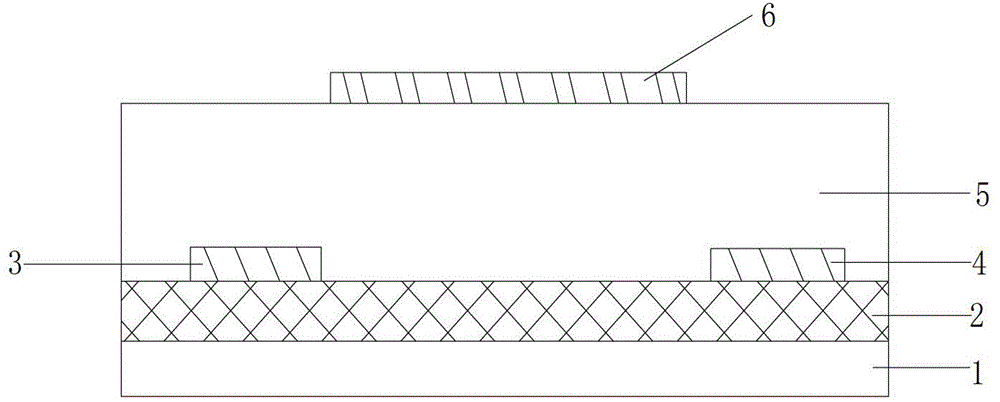
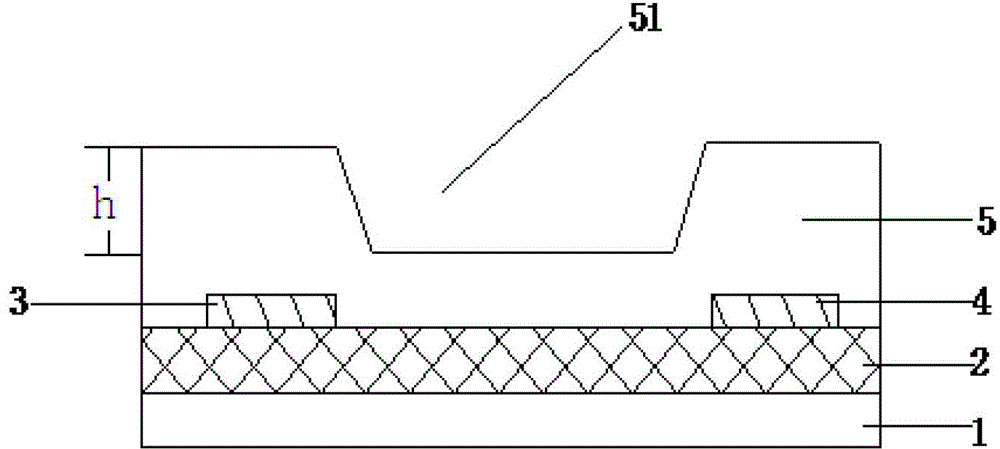
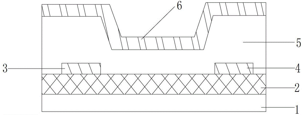
[0045] Such as Figure 2e As shown, the array substrate in the embodiment of the present invention includes: a substrate on which a thin film transistor, a passivation layer and a transparent electrode layer are sequentially arranged, a groove is formed on the tree passivation layer, and the transparent electrode layer is arranged in the groove Inside.

[0046] Specifically: a substrate 1 (a transparent substrate such as a glass substrate), on which a gate and a gate line are provided, a gate insulating layer is provided on the gate and the gate line, and an active layer, the active layer can be made of materials such as oxide semiconductor or amorphous silicon a-si, and...


PUM


Abstract

An array substrate and a manufacturing method thereof, and a display apparatus. The array substrate comprises a substrate (1). A thin film transistor, a passivation layer (5), and a transparent electrode (6) are sequentially disposed on the substrate. A groove (51) is formed on an upper surface of the passivation layer (5). The transparent electrode (6) is disposed in the groove (51).

Description

technical field [0001] The present invention relates to the field of display technology, in particular to a display device, an array substrate and a manufacturing method thereof. Background technique [0002] In recent years, with the development of science and technology, liquid crystal display technology has also been continuously improved. TFT-LCD (ThinFilmTransistor-LiquidCrystalDisplay, Thin Film Transistor-Liquid Crystal Display) occupies an important position in the display field with its advantages of good image display quality, low energy consumption, and environmental protection. TFT-LCD is formed by boxing a color filter substrate and an array substrate. Wherein, the existing array substrate usually adopts multiple masking processes to form specific structural patterns. [0003] Such as figure 1 Shown is a schematic diagram of the structure of the array substrate in the prior art. The array substrate includes a substrate 1, a gate, a gate insulating layer 2 an...

Claims


Application Information

Patent Timeline
Patent Type & Authority Patents(China)
IPC IPC(8): H01L27/12H01L21/77G02F1/1368G02F1/1343G03F7/00
CPCG02F1/134363G02F2001/133357G03F7/00H01L21/77H01L27/12H01L29/42384H01L29/4908H01L29/78606H01L29/78636H01L29/7869H01L27/1248H01L27/124G02F1/133357G02F1/133345G02F1/13439G02F1/1368H01L27/1218H01L27/1262H01L27/1288
Inventor 崔承镇刘圣烈宋泳锡
Owner BOE TECH GRP CO LTD
Features
  • R&D
  • Intellectual Property
  • Life Sciences
  • Materials
  • Tech Scout
  • Unparalleled Data Quality
  • Higher Quality Content
  • 60% Fewer Hallucinations
Learn More