Supercharge Your Innovation With Domain-Expert AI Agents!

Bump wire bonding method

A welding method and bump technology, applied in the field of bump wire bonding to improve the stability of bump wire bonding operations, can solve problems such as wire bonding failure, solder ball pull-up, and separation from pads, etc., to reduce production Cost, ease of cutting, and improved workability

Active Publication Date: 2016-04-20
SAMSUNG SEMICON CHINA RES & DEV +1
View PDF3 Cites 0 Cited by
  • Summary
  • Abstract
  • Description
  • Claims
  • Application Information

AI Technical Summary

Problems solved by technology

However, the hardness of copper wire is much higher than that of gold wire, so there are many problems in bump bonding, especially the tangent problem.
When cutting the wire at the top of the solder ball, especially when the wire has a high shear / tensile strength (for example, the wire is very thick, or copper wire), it is often because the wire is not easily cut and the wire is bonded. Failures, such as wire tails not forming properly, or solder balls being pulled off the pad

Method used


Image

  • Bump wire bonding method
  • Bump wire bonding method
  • Bump wire bonding method

Examples


Embodiment Construction

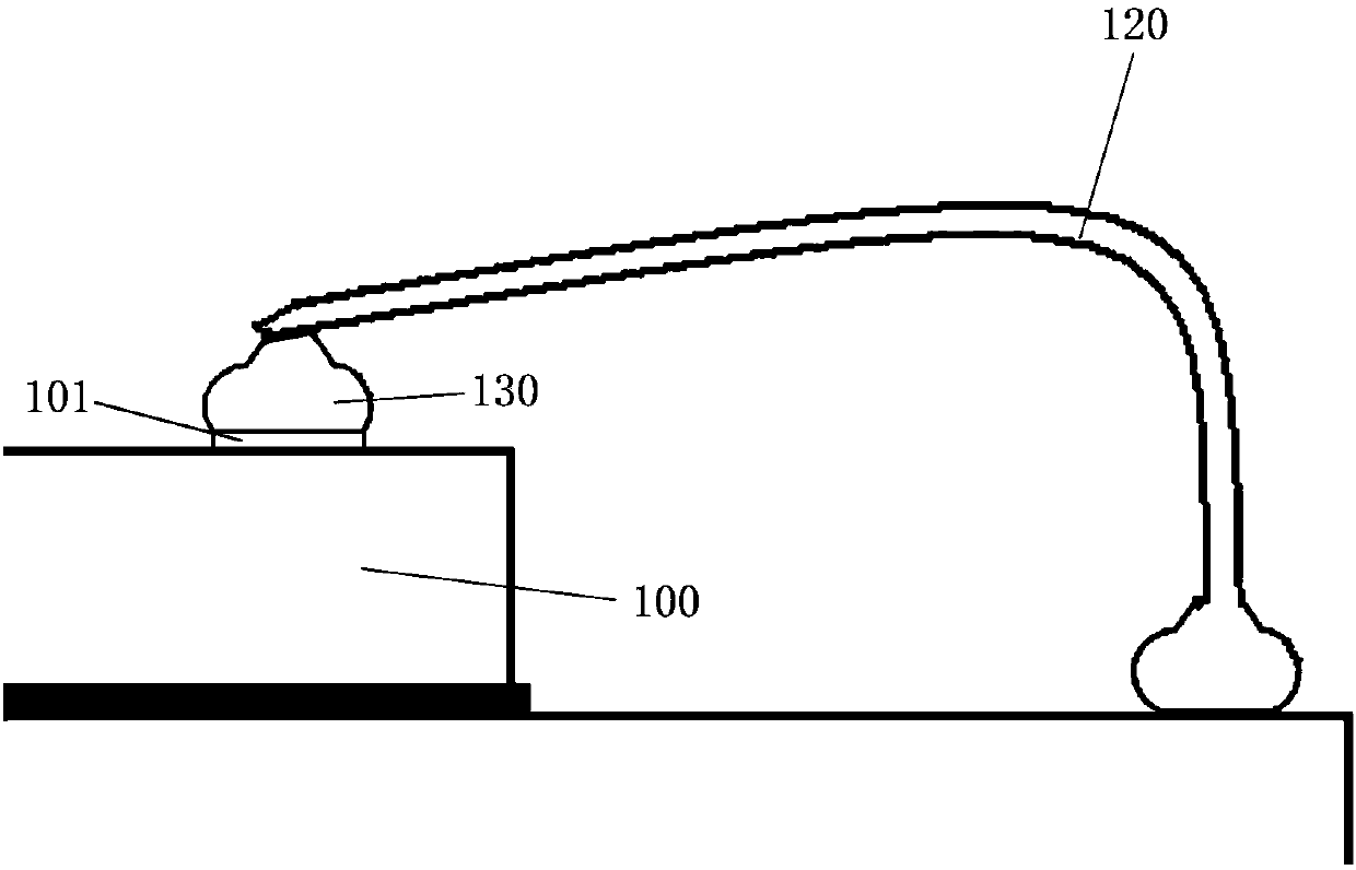
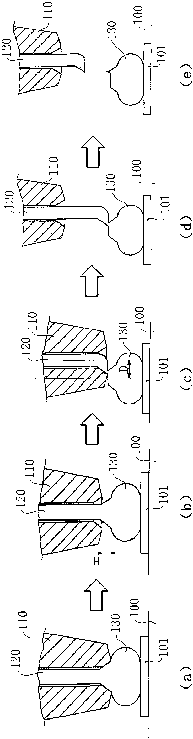
[0029] Embodiments of the invention will now be described more fully with reference to the accompanying drawings, in which exemplary embodiments of the invention are shown. However, this invention may be embodied in many different forms and should not be construed as limited to the embodiments set forth herein; rather, these embodiments are provided so that this disclosure will be thorough and complete, and will provide Those of ordinary skill in the art fully convey the concept of the embodiments of the present invention. In the following detailed description, numerous specific details are set forth by way of example in order to provide a thorough understanding of the relevant teachings. It will be apparent, however, to one skilled in the art that the present teachings may be practiced without such details. In other instances, well-known methods, procedures, components, and circuits have been described at a relatively high level and without detail in order to avoid unnecessa...


PUM


Abstract

The invention discloses a bump wire welding method. The bump wire bonding method includes: forming solder balls by a chopper and welding the solder balls to the pads; deforming the part where the solder wire and the solder balls are connected by the chopper to generate cracks; keeping the chopper vertically At the same time, the riving knife is reciprocated along the arc-shaped trajectory, so that the cracked part of the welding wire is enlarged due to the fatigue effect; the welding wire and the riving knife are clamped by the wire clamp while moving upwards in the vertical direction, pulling Break the bonding wire to complete the bump wire bonding. According to the present invention, the high-strength welding wire can be cut more easily by using the fatigue effect through multiple reciprocating movements of the riving knife, thereby improving workability while reducing production costs.

Description

technical field [0001] The invention belongs to the technical field of semiconductor packaging, in particular, the invention relates to a bump wire bonding method capable of improving the stability of the bump wire bonding operation. Background technique [0002] In order to achieve wire bonding between chips (also known as "bonding" or "bonding"), it is usually necessary to perform bump bonding first. When performing bump wire bonding, it is necessary to cut the wire on the top of the solder ball after soldering the solder ball to form a bump. [0003] figure 1 A schematic diagram of bump bonding between chips in the prior art is shown. [0004] like figure 1 As shown, in order to electrically connect the chip 100 to a substrate (not shown), a chip pad (chippad) 101 is usually provided on the chip, and then by performing a bump bonding process, a bump 130 is provided on the chip pad 101 and a Bumps (not shown) are provided on the pads (not shown) on the substrate, so as...

Claims


Application Information

Patent Timeline
Patent Type & Authority Patents(China)
IPC IPC(8): H01L21/60
CPCH01L24/48H01L2224/48H01L2224/48091H01L2224/48471H01L2224/48483H01L2224/73265H01L2224/78301H01L2224/85045H01L2924/00014H01L2924/00012H01L2224/4554
Inventor 周永华
Owner SAMSUNG SEMICON CHINA RES & DEV
Features
  • R&D
  • Intellectual Property
  • Life Sciences
  • Materials
  • Tech Scout
  • Unparalleled Data Quality
  • Higher Quality Content
  • 60% Fewer Hallucinations
Learn More