Supercharge Your Innovation With Domain-Expert AI Agents!

Electroluminescence device and manufacturing method thereof

An electroluminescent device and an organic light-emitting layer technology, applied in the direction of circuits, electrical components, electrical solid devices, etc., can solve problems such as poor contact, achieve the effects of shortening film forming time, improving product yield, and reliable connection

Active Publication Date: 2013-12-25
BOE TECH GRP CO LTD
View PDF5 Cites 8 Cited by
  • Summary
  • Abstract
  • Description
  • Claims
  • Application Information

AI Technical Summary

Problems solved by technology

[0006] Embodiments of the present invention provide an electroluminescent device and a preparation method thereof, which can improve the reliability of the electrical connection between the thin film transistor and the light emitting device, and can solve the problem of poor contact caused by impurities attached to the electrode contact surface in the prior art

Method used


Image

  • Electroluminescence device and manufacturing method thereof
  • Electroluminescence device and manufacturing method thereof
  • Electroluminescence device and manufacturing method thereof

Examples


Embodiment 1

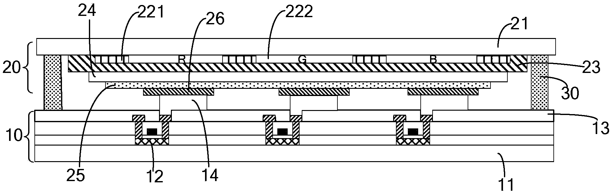
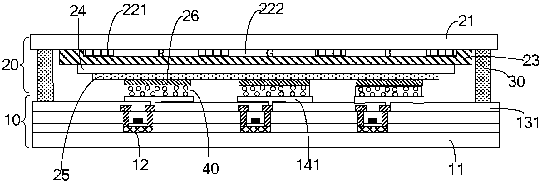
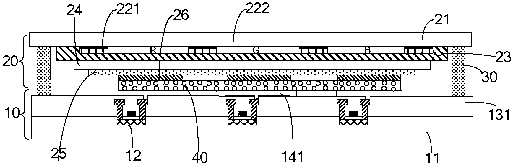
[0046] The embodiment of the present invention provides an electroluminescent device, refer to figure 2 As shown, the device includes: an array substrate 10 and a color filter substrate 20. The array substrate 10 includes: a first substrate 11, a thin film transistor 12, a first protective layer 131, and a drain connected to the thin film transistor that are sequentially disposed on the first substrate 11 The color filter substrate 20 includes: a second substrate 21, a color filter layer, a flat layer 23, a first electrode 24, an organic light-emitting layer 25, and a second electrode sequentially disposed on the second substrate 21 26. The color filter layer includes: a black matrix 221 (BM), a color resist block 222 separated by a black matrix 221 (red, green, and blue R / G / B in the figure); the second electrode 26 is connected to the first The electrodes 141 are connected together by conductive glue 40.

[0047] Generally speaking, the active electroluminescence device include...

Embodiment 2

[0062] On the other hand, this embodiment also provides a manufacturing method of an electroluminescent device, which includes: a color filter substrate manufacturing process, an array substrate manufacturing process, a color filter substrate and an array substrate aligning process, where, as Picture 10 As shown, the box-matching process of the color filter substrate and the array substrate includes:

[0063] Step 101: Apply conductive glue on the box facing surface of the color filter substrate and / or the box facing surface of the array substrate;

[0064] Step 102: align the color filter substrate with the array substrate, and heat and press the conductive adhesive during the encapsulation process, so that the second electrode and the first connecting electrode are connected together by the conductive adhesive .

[0065] Wherein, in step 101, conductive glue can be applied only to the top surface of the second electrode and / or the top surface of the first connecting electrode on ...


PUM


Abstract

The invention discloses an electroluminescence device and a manufacturing method thereof and relates to the display field. The reliability of electric connection of a thin film transistor and a second electrode is ensured, and in the meanwhile, film forming time can be shortened, the etching difficulty can be reduced and accordingly the production efficiency can be improved in the connecting electrode manufacturing process. The electroluminescence device comprises a color film substrate and an array substrate. The array substrate comprises a first substrate, a thin film transistor, a first protective layer and a first connecting electrode connected to a drain electrode of the thin film transistor, wherein the thin film transistor, the first protective layer and the first connecting electrode are sequentially arranged on the first substrate. The color film substrate comprises a second substrate, a first electrode, an organic light-emitting layer and the second electrode, wherein the first electrode, the organic light-emitting layer and the second electrode are arranged on the second substrate. The second electrode is connected with the first connecting electrode through a conductive adhesive.

Description

Technical field [0001] The invention relates to the field of display, in particular to an electroluminescence device and a preparation method thereof. Background technique [0002] Organic Light Emitting Diode (OLED), also known as Organic Electroluminescence Display (OELD), is self-luminous at the same time, does not require a backlight, high contrast, thin thickness, wide viewing angle, fast response speed, The excellent characteristics of wide operating temperature range, simple structure and manufacturing process have recently been widely used in mobile communication terminals, personal digital assistants (PDAs), handheld computers, etc. [0003] OLED devices are divided into passive matrix type and active matrix type OLED devices. The active matrix type OLED means that each OLED is controlled by a thin film transistor (TFT) circuit to control the current flowing through the OLED and has luminous efficiency. High and good image display characteristics. [0004] Such as figure 1...

Claims


Application Information

Patent Timeline
IPC IPC(8): H01L51/50H01L51/52H01L51/54H01L51/56
CPCH10K59/123H10K71/50H10K71/40H10K71/00
Inventor 程鸿飞张玉欣
Owner BOE TECH GRP CO LTD
Features
  • R&D
  • Intellectual Property
  • Life Sciences
  • Materials
  • Tech Scout
  • Unparalleled Data Quality
  • Higher Quality Content
  • 60% Fewer Hallucinations
Learn More